
User's Manual
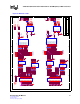
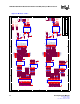
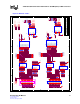
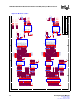
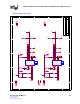
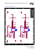
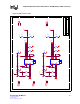
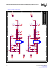
Table Of Contents
- 1.0 General Description
- 2.0 Introduction
- 3.0 Quick-Start Checklist
- 4.0 Optional Configurations
- 5.0 LEDs
- 6.0 Board Schematics
- Figure 4. LXD9785 PQFP MII Demo Board Power (Fiber Board Revision A2)
- Figure 5. Control
- Figure 6. MII Ports 0 and 1
- Figure 7. MII Ports 2 and 3
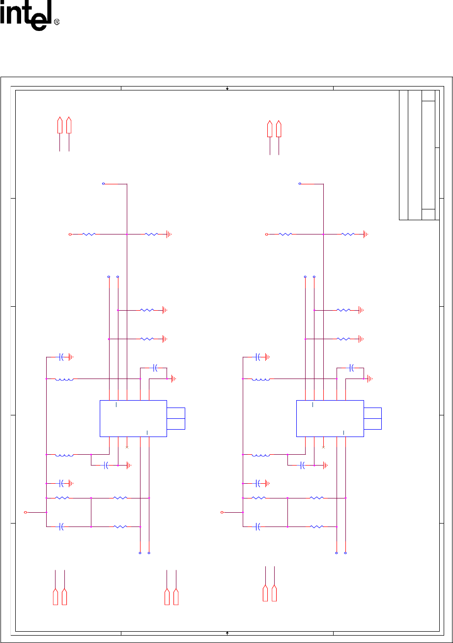
- Figure 8. MII Ports 4 and 5
- Figure 9. MII Ports 6 and 7
- Figure 10. Fiber Ports 0 and 1
- Figure 11. Fiber Ports 2 and 3
- Figure 12. Fiber Ports 4 and 5
- Figure 13. Fiber Ports 6 and 7
- Figure 14. Caps
- Figure 15. SS-SMII to MII ALTERA
- Figure 16. Clock Distribution
- Figure 17. Inter-Frame Status LEDs
- Figure 18. Logic Analyzer
- Figure 19. MDIO0 and MDC0 Fix
- Figure 20. MDIO1 and MDC1 Fix
- 7.0 Bill of Materials
LXD9785 PQFP Demo Board with FPGA for SS-SMII (Fiber)-to-MII Conversion
Development Kit Manual 27
Document #: 249323
Revision #: 003
Rev. Date: January 24, 2002
Figure 12. Fiber Ports 4 and 5
A
A
B
B
C
C
D
D
E
E
4 4
3 3
2 2
1 1
FIBER PORTS 4&5 A2
LXD9785 SS/SMII MII FX DV BOARD
B
10 18Wednesday, February 21, 2001
Title
Size Document Number Rev
Date: Sheet
of
TPFIP4
TPFIN4
TPFIP5
TPFIN5
TPFOP4
TPFON4
TPFON5
TPFOP5
TPFON4
TPFOP4
TPFIP4
TPFIN4
TPFIN5
TPFIP5
TPFON5
TPFOP5
SD5
SD4
SD4
SD5
TPFIN4 6
TPFIP4 6
TPFIN5 6
TPFIP5 6
TPFON46
TPFOP46
TPFOP56
TPFON56
SD56
SD46
GND
GNDGND
GND
GND GND
GND
GND
GND
GND
GND
GND
GND
GND
VCC_FX
VCC_FX
VCC_FX
VCC_FX
+
C303
0.1uF
R700
50 1%
TP214
1
R691
50 1%
+
C307
0.1uF
TP212
1
R690
50 1%
R702
130
TP213
1
+
C300
10uF
+
C301
0.1uF
R694
82
FIBER PORT
F5
HFBR_5903
6
7
8
9
10
5
4
3
2
1
TX Vcc
TX Gnd
N/C
TD
TD
RD
RD
SD
RX Vcc
RX Gnd
R703
82
FIBER PORT
F6
HFBR_5903
6
7
8
9
10
5
4
3
2
1
TX Vcc
TX Gnd
N/C
TD
TD
RD
RD
SD
RX Vcc
RX Gnd
R696
130
R701
130
TP188
1
+
C305
0.1uF
TP189
1
L10
1uH
R687
130
+
C311
0.1uF
R686
27
+
C306
10uF
R695
27
+
C310
0.1uF
TP208
1
R692
130
L11
1uH
TP209
1
R693
130
+
C309
0.1uF
TP211
1
L9
1uH
L12
1uH
TP210
1
+
C304
0.1uF
R699
50 1%
TP215
1