
User's Manual
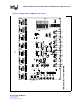
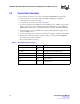
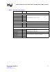
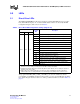
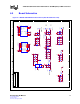
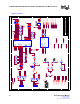
Table Of Contents
- 1.0 General Description
- 2.0 Introduction
- 3.0 Quick-Start Checklist
- 4.0 Optional Configurations
- 5.0 LEDs
- 6.0 Board Schematics
- Figure 4. LXD9785 PQFP MII Demo Board Power (Fiber Board Revision A2)
- Figure 5. Control
- Figure 6. MII Ports 0 and 1
- Figure 7. MII Ports 2 and 3
- Figure 8. MII Ports 4 and 5
- Figure 9. MII Ports 6 and 7
- Figure 10. Fiber Ports 0 and 1
- Figure 11. Fiber Ports 2 and 3
- Figure 12. Fiber Ports 4 and 5
- Figure 13. Fiber Ports 6 and 7
- Figure 14. Caps
- Figure 15. SS-SMII to MII ALTERA
- Figure 16. Clock Distribution
- Figure 17. Inter-Frame Status LEDs
- Figure 18. Logic Analyzer
- Figure 19. MDIO0 and MDC0 Fix
- Figure 20. MDIO1 and MDC1 Fix
- 7.0 Bill of Materials
LXD9785 PQFP Demo Board with FPGA for SS-SMII (Fiber)-to-MII Conversion
12 Development Kit Manual
Document #: 249323
Revision #: 003
Rev. Date: January 24, 2002
3.0 Quick-Start Checklist
Use this quick-start procedure for easy setup of the LXD9785 PQFP MII Demo Board. This
procedure sets all ports to the default condition (100 Mbps and full-duplex capabilities).
1. Set the jumpers in accordance with Table 1.
2. Set switches S1, S5, and S8 in accordance with Table 2.
3. Connect the eight Demo Board MII ports to the SmartBits test box via MII connector/cables.
Male-to- male connectors are required to interface the SmartBits test box to the LXD9785
PQFP MII Demo Board and are available from Newark (.5m cable - Newark P/N 91F9746).
4. Connect the fiber ports to external NIC cards via fiber cables. Each NIC card plugs directly
into the SmartBits test box.
5. Connect +2.5V DC power to VCC and a +3.3V DC power supply to VCCIO and VCC-EXT.
6. With the Demo Board appropriately configured, apply power to the LXD9785 PQFP MII
Demo Board and press Reset switch S4.
7. Proceed with evaluation as desired.
Table 1. Quick-Start Jumper Settings
Jumper / Label Setting Configuration
JP1 / MDIO
Jumper Pins
2 & 3
Routes MDIO through Port 0 MII Connector.
JP2 / MDC
Jumper Pins
2 & 3
Routes MDC through Port 0 MII Connector.
JP12 / SD Interface Open Enables 3.3V SD Fiber interface.
JP13 Jumpered Provides voltage to Fiber transceivers.
JP15
Jumper Pins
2 & 3
Enables 1x8 mode.
JP16
Jumper Pins
1 & 2
Enables 2x4 mode.