R Intel® 845 Chipset: 82845 Memory Controller Hub (MCH) for SDR Datasheet January 2002 Document Number: 290725-002
R ® Information in this document is provided in connection with Intel products. No license, express or implied, by estoppel or otherwise, to any intellectual property rights is granted by this document.
R Contents 1 Introduction ........................................................................................................................11 1.1 1.2 1.3 1.4 2 Terminology and Notations ...................................................................................11 Reference Documents ..........................................................................................13 ® Intel 845 Chipset System Architecture ................................................................
R 3.5 3.6 4 Host-Hub Interface Bridge Device Registers (Device 0)......................................43 3.5.1 VID—Vendor Identification Register (Device 0) ....................................45 3.5.2 DID—Device Identification Register (Device 0).....................................45 3.5.3 PCICMD—PCI Command Register (Device 0) .....................................46 3.5.4 PCISTS—PCI Status Register (Device 0).............................................47 3.5.
R 3.6.11 3.6.12 3.6.13 3.6.14 3.6.15 3.6.16 3.6.17 3.6.18 3.6.19 3.6.20 3.6.21 3.6.22 3.6.23 3.6.24 4 SBUSN1—Secondary Bus Number Register (Device 1) ......................86 SUBUSN1—Subordinate Bus Number Register (Device 1)..................86 SMLT1—Secondary Master Latency Timer Register (Device 1) .........87 IOBASE1—I/O Base Address Register (Device 1) ...............................88 IOLIMIT1—I/O Limit Address Register (Device 1) ................................
R 5.3 5.4 5.5 5.6 6 Electrical Characteristics .................................................................................................119 6.1 6.2 6.3 6.4 7 Package Mechanical Information........................................................................134 Testability.........................................................................................................................137 8.1 8.2 6 Absolute Maximum Ratings ............................................................
R Figures ® Figure 1. Intel MCH Simplified Block Diagram.................................................................20 Figure 2. PAM Register Attributes .....................................................................................60 Figure 3. Addressable Memory Space ..............................................................................97 Figure 4. DOS Compatible Area Address Map..................................................................98 Figure 5.
R Revision History Revision Number Description Date -001 Initial Release. September 2001 -002 • Changed the document name to add the term “for SDR”. January 2002 • DWTC—DRAM Write Thermal Management Control Register was incorrectly placed in Device 0. It should be in Device 1. • DRTC—DRAM Read Thermal Management Control Register was incorrectly placed in Device 0. It should be in Device 1.
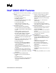
R Intel® 82845 MCH Features ! Intel® Pentium® 4 Processor (478 pin package) ! Accelerated Graphics Port (AGP) Interface ! ! ! ® Support Enhanced Mode Scaleable Bus Protocol 2x Address, 4x Data System Bus interrupt delivery 400 MHz system bus System Bus Dynamic Bus Inversion (DBI) 32-bit system bus addressing 12 deep In-Order Queue AGTL+ bus driver technology with integrated AGTL+ termination resistors System Memory Support Directly supports one SDR SDRAM channel, 64 bits wide (72 bi
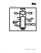
R System Block Diagram Intel ® Pentium ® 4 Processor Intel ® 845 Chipset System Memory 4x AGP Graphics Controller AGP 2.0 Intel ® 82845 Memory Controller Hub (MCH) SDRAM Interface SDRAM Hub Interface 2 IDE Drives PCI Slots UltraATA/100 PCI Bus 4 USB Ports; 2 HC AC '97 Codec(s) (optional) AC'97 2.
Introduction R 1 Introduction The Intel® 82845 Memory Controller Hub (MCH) is designed for use with the Intel® Pentium® 4 processor in the 478-pin package. The Intel® 845 chipset contains two main components: the 82845 Memory Controller Hub (MCH) for the host bridge and the Intel 82801BA I/O Controller Hub (ICH2) for the I/O subsystem. The MCH provides the processor interface, system memory interface, AGP interface, and hub interface in an 845 chipset desktop platform.
Introduction R Term Description GART Graphics Aperture Re-map Table. This table contains the page re-map information used during AGP aperture address translations. GTLB Graphics Translation Look-aside Buffer. A cache used to store frequently used GART entries. UP Uni-Processor. DBI Dynamic Bus inversion. MSI Message Signaled Interrupts. MSIs allow a device to request interrupt service via a standard memory write transaction instead of through a hardware signal. IPI Inter Processor Interrupt.
Introduction R 1.2 Reference Documents Document Document Number / Location Intel® Pentium 4 Processor in a 478 Pin Package and Intel® 845 Chipset Platform for SDR Design Guide 298354 Intel® 82801BA I/O Controller Hub (ICH2) and Intel® 82801BAM I/O Controller Hub (ICH2-M) Datasheet 290687 Intel® 845 Chipset Thermal and Mechanical Design Guidelines for SDR 298586 ® Intel 82802AB/AC Firmware Hub (FWH) Datasheet 290658 PCI Local Bus Specification, Revision 2.
Introduction R 1.3 Intel® 845 Chipset System Architecture The MCH provides the processor interface, system memory interface, AGP interface, and hub interface in an 845 chipset desktop platform. The processor interface supports the Pentium 4 processor subset of the Extended Mode of the Scalable Bus Protocol. The MCH supports a single channel of PC133 SDRAM. The MCH contains advanced power management logic.
Introduction R 1.4.1 System Bus Interface The MCH is optimized for the Pentium 4 processor. The primary enhancements over the Compatible Mode P6 bus protocol are: • Source synchronous double-pumped address • Source synchronous quad-pumped data • System bus interrupt and side-band signal delivery The MCH supports a 64-byte cache line size. Only one processor is supported at a system bus frequency of 400 MHz. The MCH supports a 3:4 host-to-memory frequency ratio (using the 100 MHz clock).
Introduction R 1.4.3 System Memory Interface The MCH directly supports one channel of PC133 SDRAM. The memory interface supports Single Data Rate (SDR) devices with densities of 64 Mb, 128 Mb, 256 Mb, and 512 Mb technology. The memory interface also supports variable page sizes of 2 KB, 4 KB, 8 KB, and 16 KB. Page size is individually selected for every row and a maximum of 8 pages per DIMM may be opened simultaneously.
Introduction R 1.4.5 Hub Interface The 8-bit hub interface connects the MCH to the ICH2. All communication between the MCH and the ICH2 occurs over the hub interface. The hub interface runs at 66 MHz / 266 MB/s. In addition to the normal traffic types, the following communication also occurs over the hub interface: • Interrupt related messages • Power management events as messages • SMI, SCI, and SERR error indication messages It is assumed that the hub interface is always connected to an ICH2. 1.4.
Introduction R 1.4.7 System Interrupts The MCH supports both Intel 8259 and Pentium 4 processor interrupt delivery mechanisms. The serial APIC interrupt mechanism is not supported. Intel 8259 support consists of flushing inbound hub interface write buffers when an Interrupt Acknowledge cycle is forwarded from the system bus to the hub interface. The MCH supports the Pentium 4 processor interrupt delivery mechanism. IOxAPIC and PCI MSI interrupts are generated as memory writes.
Signal Description R 2 Signal Description This chapter provides a detailed description of the MCH signals. The signal descriptions are arranged in functional groups according to their associated interface (see Figure 1). The states of all of the signals during reset are provided in the System Reset section. The “#” symbol at the end of a signal name indicates that the active, or asserted state occurs when the signal is at a low voltage level.
Signal Description R ® Figure 1.
Signal Description R 2.1 System Bus Signals Signal Name Type Description ADS# I/O AGTL+ Address Strobe: The system bus owner asserts ADS# to indicate the first of two cycles of a request phase. BNR# I/O AGTL+ Block Next Request: BNR# is used to block the current request bus owner from issuing a new request. This signal dynamically controls the system bus pipeline depth. BPRI# O AGTL+ Bus Priority Request: The MCH is the only Priority Agent on the system bus.
Signal Description R Signal Name Type Description HD[63:0]# I/O AGTL+ Host Data: These signals are connected to the system data bus. HD[63:0]# are transferred at a 4x rate. Note that the data signals are inverted on the system bus. HDSTBP[3:0]# I/O AGTL+ Differential Host Data Strobes: The differential source synchronous strobes used to transfer HD[63:0]# and DBI[3:0]# at the 4x transfer rate.
Signal Description R 2.2 SDR SDRAM Interface Signals Signal Name SCS[11:0]# Type O CMOS Description Chip Select: These signals select the particular SDRAM components during the active state. Note: There are two SCS# signals per SDRAM row. These signals can be toggled on every rising system memory clock edge. 2.3 SMA[12:0] O CMOS Multiplexed Memory Address: These signals are used to provide the multiplexed row and column address to SDRAM.
Signal Description R 2.4 AGP Interface Signals 2.4.1 AGP Addressing Signals Signal Name PIPE# Type Description I AGP Pipelined Read: This signal is asserted by the AGP master to indicate a full-width address is to be enqueued on by the target using the AD bus. One address is placed in the AGP request queue on each rising clock edge while PIPE# is asserted. When PIPE# is deasserted, no new requests are queued across the AD bus. During SBA Operation: Not Used. During FRAME# Operation: Not Used.
Signal Description R 2.4.2 AGP Flow Control Signals Signal Name RBF# Type Description I AGP Read Buffer Full: RBF# indicates if the master is ready to accept previously requested low priority read data. When RBF# is asserted, the MCH is not allowed to initiate the return low priority read data. That is, the MCH can finish returning the data for the request currently being serviced. RBF# is only sampled at the beginning of a cycle.
Signal Description R 2.4.4 AGP Strobes Signals Signal Name 2.4.5 Type Description AD_STB0 I/O (s/t/s) AGP Address/Data Bus Strobe-0: This signal provides timing for 2x and 4x data on AD[15:0] and the C/BE[1:0]# signals. The agent that is providing the data drives this signal. AD_STB0# I/O (s/t/s) AGP Address/Data Bus Strobe-0 Compliment: Differential strobe pair that provides timing information for the AD[15:0] and C/BE[1:0]# signals. The agent that is providing the data drives this signal.
Signal Description R Signal Name Type Description G_DEVSEL# I/O s/t/s AGP Device Select: This signal indicates that a FRAME#-based AGP target device has decoded its address as the target of the current access. The MCH asserts G_DEVSEL# based on the DRAM address range being accessed by a PCI initiator. As an input it indicates whether any device on the bus has been selected. G_REQ# I AGP Request: Indicates that a FRAME# or PIPE#-based AGP master is requesting use of the AGP interface.
Signal Description R 2.5 Clocks, Reset, and Miscellaneous Signals Signal Name BCLK BCLK# 66IN Type Description I CMOS Differential Host Clock In: These pins receive a differential host clock from the external clock synthesizer. This clock is used by all of the MCH logic that is in the host clock domain. I CMOS 66 MHz Clock In: This pin receives a 66 MHz clock from the clock synthesizer. This clock is used by AGP/PCI and hub interface clock domains. Note: That this clock input is 3.3 V tolerant.
Signal Description R 2.6 Voltage Reference and Power Signals Signal Name ® Type Description HVREF Ref Host Reference Voltage: Reference voltage input for the data, address, and common clock signals of the host AGTL+ interface. SDREF Ref SDRAM Reference Voltage: Reference voltage input for DQ, DQS, RDCLKIN (SDR). HI_REF Ref Hub Interface Reference: Reference voltage input for the hub interface. AGPREF Ref AGP Reference: Reference voltage input for the AGP interface.
Signal Description R 2.
Register Description R 3 Register Description The MCH contains two sets of software accessible registers, accessed via the host processor I/O address space: • Control registers I/O mapped into the processor I/O space, which control access to PCI and AGP configuration space (see Section 3.3). • Internal configuration registers residing within the MCH are partitioned into two logical device register sets (“logical” since they reside within a single physical device).
Register Description R Term 3.2 Description Reserved Registers In addition to reserved bits within a register, the MCH contains address locations in the configuration space that are marked “Reserved”. When a “Reserved” register location is read, a random value is returned. (“Reserved” registers can be 8-, 16-, or 32-bit in size). Registers that are marked as “Reserved” must not be modified by system software. Writes to “Reserved” registers may cause system failure.
Register Description R 3.2.1 Standard PCI Bus Configuration Mechanism The PCI Bus defines a slot based "configuration space" that allows each device to contain up to 8 functions with each function containing up to 256 8-bit configuration registers. The PCI specification defines two bus cycles to access the PCI configuration space: Configuration Read and Configuration Write. Memory and I/O spaces are supported directly by the processor.
Register Description R Primary PCI and Downstream Configuration Mechanism If the Bus Number in the CONF_ADDR is non-zero, and is less than the value in the Host-AGP device’s Secondary Bus Number register, or greater than the value in the Host-AGP device’s Subordinate Bus Number register, the MCH will generate a Type 1 hub interface configuration cycle.
Register Description R Bit 31 Descriptions Configuration Enable (CFGE). 0 = Disable. 1 = Enable. Accesses to PCI configuration space are enabled. 30:24 Reserved. These bits are read only and have a value of 0. 23:16 Bus Number. When Bus Number is programmed to 00h, the target of the configuration cycle is a hub interface agent (MCH, ICH2, etc.). The configuration cycle is forwarded to the hub interface, if Bus Number is programmed to 00h and the MCH is not the target (the device number is ≥2).
Register Description R 3.3.2 CONF_DATA—Configuration Data Register I/O Address: Default Value: Access: Size: 0CFCh 00000000h R/W 32 bits CONF_DATA is a 32 bit read/write window into configuration space. The portion of configuration space that is referenced by CONF_DATA is determined by the contents of CONF_ADDR. 3.4 Bit Descriptions 31:0 Configuration Data Window (CDW).
Register Description R 3.4.1 DRAMWIDTH—DRAM Width Register Address Offset: Default Value: Access: Size: 2Ch 00h R/W 8 bits This register determines the width of SDRAM devices populated in each row of memory. Bit 7:6 Descriptions Reserved. 5 Row 5 Width. Width of devices in Row 5 0 = 16-bit wide devices, or Unpopulated (default) 1 = 8-bit wide devices 4 Row 4 Width. Width of devices in Row 4 0 = 16-bit wide devices, or Unpopulated (default) 1 = 8-bit wide devices 3 Row 3 Width.
Register Description R 3.4.2 DQCMDSTR—Strength Control Register (SDQ and CMD Signal Groups) Memory Address Offset: Default Value: Access: Size: 30h 00h R/W 8 bits This register controls the drive strength of the I/O buffers for the DQ/DQS and CMD signal groups. Bit 7 6:4 Descriptions Reserved. CMD Strength Control (SRAS#, SCAS#, SWE#, SMA[12:0], SBS[1:0]). This field selects the signal drive strength. 000 = 0.75 X (default) 001 = 1.00 X 010 = 1.25 X 011 = 1.50 X 100 = 2.00 X 101 = 2.50 X 110 = 3.
Register Description R 3.4.3 CKESTR—Strength Control Register (SCKE Signal Group) Memory Address Offset: Default Value: Access: Size: 31h 00h R/W 8 bits This register controls the drive strength of the I/O buffers for the CKE signal group. This group has two possible loadings depending on the width of SDRAM devices used in each row of memory (x8 or x16). The proper strength can be independently programmed for each configuration.
Register Description R 3.4.4 CSBSTR—Strength Control Register (SCS# Signal Group) Memory Address Offset: Default Value: Access: Size: 32h 00h R/W 8 bits This register controls the drive strength of the I/O buffers for the SCS# signal group. This group has two possible loadings depending on the width of SDRAM devices used in each row of memory (x8 or x16). The proper strength can be independently programmed for each configuration.
Register Description R 3.4.5 CKSTR—Strength Control Register (Clock Signal Group) Memory Address Offset: Default Value: Access: Size: 33h 00h R/W 8 bits This register controls the drive strength of the I/O buffers for the Clock (CK) signal group including both the CK and CK# signals. This group has two possible loadings depending on the width of SDRAM devices used in each row of memory (x8 or x16). The proper strength can be independently programmed for each configuration.
Register Description R 3.4.6 RCVENSTR—Strength Control Register (RCVENOUT Signal Group) Memory Address Offset: Default Value: Access: Size: 34h 00h R/W 8 bits This register controls the drive strength of the I/O buffers for the Receive Enable Out signal group (RDCLKO# signal). Bit Descriptions 7:3 Reserved. 2:0 Receive Enable Out Signal Group (RCVEnOut) Strength Control. This field selects the signal drive strength. 000 = 0.75 X (default) 001 = 1.00 X 010 = 1.25 X 011 = 1.50 X 100 = 2.00 X 101 = 2.
Register Description R 3.5 Host-Hub Interface Bridge Device Registers (Device 0) Table 8 provides the register address map for Device 0 PCI configuration space. An “s” in the Default Value column indicates that a strap determines the power-up default value for that bit. ® Table 8.
Register Description R Address Offset Register Symbol 87–8Bh — 8C–8Fh EAP 90–96h PAM[0:6] 97h FDHC 98–9Ch — 9Dh SMRAM 9Eh ESMRAMC 9Fh — A0–A3h ACAPID A4–A7h Default Value Access Reserved. — — Error Address Pointer 00000000h RO Programmable Attribute Map (7 Registers) 0000000000 0000h RO, R/W Fixed DRAM Hole Control 00h R/W Reserved. — — System Management RAM Control 02h RO, R/W, R/W/L Extended System Mgmt RAM Control 38h RO, R/W, R/WC, R/W/L Reserved.
Register Description R 3.5.1 VID—Vendor Identification Register (Device 0) Address Offset: Default Value: Attribute: Size: 00–01h 8086h RO 16 bits The VID Register contains the vendor identification number. This 16-bit register combined with the DID Register uniquely identifies any PCI device. Writes to this register have no effect. Bit 15:0 Description Vendor Identification Number. This is a 16-bit value assigned to Intel. Intel VID = 8086h. 3.5.
Register Description R 3.5.3 PCICMD—PCI Command Register (Device 0) Address Offset: Default: Access: Size 04–05h 0006h R/W, RO 16 bits Since MCH Device 0 does not physically reside on PCI0, many of the bits are not implemented. Bit 15:10 Descriptions Reserved. 9 Fast Back-to-Back—RO. Not implemented; Hardwired to 0. This bit controls whether or not the master can do fast back-to-back write. Since device 0 is strictly a target this bit is not implemented. 8 SERR Enable (SERRE)—R/W.
Register Description R 3.5.4 PCISTS—PCI Status Register (Device 0) Address Offset: Default Value: Access: Size: 06–07h 0090h RO, R/WC 16 bits PCISTS is a 16-bit status register that reports the occurrence of error events on Device 0s on the hub interface. Since MCH Device 0 is the Host-to-hub interface bridge, many of the bits are not implemented. Bit Description 15 Reserved. 14 Signaled System Error (SSE)—R/WC. 0 = Software clears this bit by writing a 1 to it.
Register Description R 3.5.5 RID—Revision Identification Register (Device 0) Address Offset: Default Value: Access: Size: 08h See table below RO 8 bits This register contains the revision number of the MCH Device 0. These bits are read only and writes to this register have no effect. Bit Description 7:0 Revision Identification Number. This is an 8-bit value that indicates the revision identification number for the MCH Device 0. 03h = A3 Stepping 04h = B0 Stepping 3.5.
Register Description R 3.5.8 MLT—Master Latency Timer Register (Device 0) Address Offset: Default Value: Access: Size: 0Dh 00h RO 8 bits The hub interface does not comprehend the concept of Master Latency Timer. Therefore, this register is not implemented. Bit 7:0 3.5.9 Description Hardwired to 00h. Writes have no effect. HDR—Header Type Register (Device 0) Address Offset: Default: Access: Size: 0Eh 00h RO 8 bits This register identifies the header layout of the configuration space.
Register Description R 3.5.10 APBASE—Aperture Base Configuration Register (Device 0) Offset: Default: Access: Size: 10–13h 0000_0008h R/W, RO 32 bits The APBASE is a standard PCI Base Address register that is used to set the base of the Graphics Aperture. The standard PCI Configuration mechanism defines the base address configuration register such that only a fixed amount of space can be requested (dependent on which bits are hardwired to 0 or behave as hardwired to 0).
Register Description R 3.5.11 SVID—Subsystem Vendor Identification (Device 0) Offset: Default: Access: Size: 2C–2Dh 0000h R/WO 16 bits This value is used to identify the vendor of the subsystem. Bit 15:0 3.5.12 Description Subsystem Vendor ID. (Default = 0000h). This field should be programmed during boot-up. After this field is written once, it becomes read only.
Register Description R 3.5.14 AGPM—AGP Miscellaneous Configuration Register (Device 0) Address Offset: Default Value: Access: Size: Bit 7:2 1 3.5.15 51h 00h R/W 8 bits Descriptions Reserved. Aperture Access Global Enable (APEN). This bit is used to prevent access to the graphics aperture from any port (processor, hub interface, or AGP/PCI_B) before the aperture range is established by the configuration software and the appropriate translation table in system memory has been initialized.
Register Description R 3.5.16 DRA—DRAM Row Attribute Registers (Device 0) Offset: Default: Access: Size: 70–73h (DRA0–DRA3) 00h R/W 8 bits The DRAM Row Attribute Register defines the page sizes to be used when accessing different pairs of rows.
Register Description R Bit 7 6:4 Description Reserved. Row Attribute for Odd-Numbered Row (RAODD). This 3-bit field defines the page size of the corresponding row. 001 = 2 KB 010 = 4 KB 011 = 8 KB 100 = 16 KB Others = Reserved 3 Reserved. 2:0 Row Attribute for Even-Numbered Row (RAEVEN). This 3-bit field defines the page size of the corresponding row.
Register Description R 3.5.17 DRT—DRAM Timing Register (Device 0) Offset: Default: Access: Size: 78–7Bh 00000010h R/W 32 bits Bit Description 31:19 Reserved. 18:16 DRAM Idle Timer. This field determines the number of clocks the DRAM controller will remain in the idle state before it begins precharging all pages. 000 = infinite. 001 = 0 DRAM clocks 010 = 8 DRAM clocks 011 = 16 DRAM clocks 100 = 64 DRAM clocks Others = Reserved 15:11 Reserved. 10:9 Activate to Precharge delay (tRAS).
Register Description R 3.5.18 DRC—DRAM Controller Mode Register (Device 0) Offset: Default: Access: Size: 7C–7Fh 00000000h R/W, RO 32 bits Bit Description 31:30 Revision Number (REV)—R/W. Reflects the revision number of the format used for SDRAM register definition. Currently, this field must be 00, since this revision (rev 00) is the only existing version of the specification. 29 Initialization Complete (IC)—R/W.
Register Description R Bit 6:4 Description Mode Select (SMS)—R/W. These bits select the special operational mode of the system memory interface. The special modes are intended for initialization at power up. 000 = Post Reset state. When the MCH exits reset (power-up or otherwise), the mode select field is cleared to “000”. During any reset sequence, while power is applied and reset is active, the MCH asserts all CKE signals.
Register Description R 3.5.19 DERRSYN—DRAM Error Syndrome Register (Device 0) Address Offset: Default Value: Access: Size: 86h 00h RO 8 bits This register is used to report the ECC syndromes for each quadword of a 32 byte-aligned data quantity read from the system memory array. Bit 7:0 Description DRAM ECC Syndrome (DECCSYN). After a system memory ECC error, hardware loads this field with a syndrome that describes the set of bits found to be in error.
Register Description R 3.5.21 PAM[0:6]—Programmable Attribute Map Registers (Device 0) Address Offset: Default Value: Attribute: Size: 90–96h (PAM0–PAM6) 00h R/W, RO 8 bits The MCH allows programmable memory attributes on 13 Legacy memory segments of various sizes in the 640 Kbytes to 1 Mbytes address range. Seven Programmable Attribute Map (PAM) Registers are used to support these features. Cacheability of these areas is controlled via the MTRR registers in the processor.
Register Description R At the time that a hub interface or AGP accesses to the PAM region may occur, the targeted PAM segment must be programmed to be both readable and writeable. As an example, consider BIOS that is implemented on the expansion bus. During the initialization process, the BIOS can be shadowed in system memory to increase the system performance. When BIOS is shadowed in system memory, it should be copied to the same address location.
Register Description R Table 9.
Register Description R Extended System BIOS Area (E0000h–EFFFFh) This 64 KB area is divided into four 16 KB segments that can be assigned with different attributes via PAM control register as defined by the table above. System BIOS Area (F0000h–FFFFFh) This area is a single 64 KB segment, which can be assigned with different attributes via PAM control register as defined by the table above. 3.5.
Register Description R 3.5.23 SMRAM—System Management RAM Control Register (Device 0) Address Offset: Default Value: Access: Size: 9Dh 02h R/W, RO, R/W/L 8 bits The SMRAMC register controls how accesses to Compatible and Extended SMRAM spaces are treated. The Open, Close, and Lock bits function only when the G_SMRAME bit is set to a 1. Also, the OPEN bit must be reset before the LOCK bit is set. Bit Description 7 Reserved. 6 SMM Space Open (D_OPEN)—R/W/L.
Register Description R 3.5.24 ESMRAMC—Extended System Mgmt RAM Control Register (Device 0) Address Offset: Default Value: Access: Size: 9Eh 38h RO, R/W, R/WC, R/W/L 8 bits The Extended SMRAM register controls the configuration of Extended SMRAM space. The Extended SMRAM (E_SMRAM) memory provides a write-back cacheable SMRAM memory space that is above 1 MB. Bit Description 7 H_SMRAM_EN (H_SMRAME)—R/W/L. Controls the SMM memory space location (i.e., above 1 MB or below 1 MB).
Register Description R 3.5.25 ACAPID—AGP Capability Identifier Register (Device 0) Address Offset: Default Value: Access: Size: A0–A3h 0020_0002h RO 32 bits This register provides standard identifier for AGP capability. Bit Description 31:24 Reserved. 23:20 Major AGP Revision Number (MAJREV). These bits provide a major revision number of AGP specification that this version of the MCH conforms. This field is hardwired to value of “0010b” (i.e., implying Rev 2.x).
Register Description R 3.5.26 AGPSTAT—AGP Status Register (Device 0) Address Offset: Default Value: Access: Size: A4–A7h 1F00_0217h RO 32 bits This register reports AGP device capability/status. Bit 31:24 Description Request Queue (RQ). This field contains the maximum number of AGP command requests the MCH is configured to manage. 1Fh = Allows a maximum of 32 outstanding AGP command requests. 23:10 9 8:6 Reserved. Side Band Addressing Support (SBA).
Register Description R 3.5.27 AGPCMD—AGP Command Register (Device 0) Address Offset: Default Value: Access: Size: A8–ABh 0000_0000h R/W 32 bits This register provides control of the AGP operational parameters. Bit 31:10 9 Description Reserved. SideBand Address Enable (SBAEN). 0 = Disable. 1 = Enable. 8 AGP Enable (AGPEN). 0 = The MCH ignores all AGP operations, including the sync cycle. Any AGP operation received while this bit is 1 will be serviced, even if this bit is set to 0.
Register Description R 3.5.28 AGPCTRL—AGP Control Register (Device 0) Address Offset: Default Value: Access: Size: B0–B3h 0000_0000h R/W 32 bits This register provides for additional control of the AGP interface. Bit 31:8 7 Description Reserved. GTLB Enable (GTLBEN). This bit provides enable and flush control of the GTLB. 0 =Disable (Default). GTLB is flushed by clearing the valid bits associated with each entry. 1 =Enable. Normal operations of the Graphics Translation Lookaside Buffer.
Register Description R 3.5.29 APSIZE—Aperture Size (Device 0) Address Offset: Default Value: Access: Size: B4h 00h R/W 8 bits This register determines the effective size of the Graphics Aperture used for a particular MCH configuration. This register can be updated by the MCH specific BIOS configuration sequence before the PCI standard bus enumeration sequence takes place. If the register is not updated, the default value will select an aperture of maximum size (i.e., 256 MB).
Register Description R 3.5.30 ATTBASE—Aperture Translation Table Base Register (Device 0) Address Offset: Default Value: Access: Size: B8–BBh 0000_0000h R/W 32 bits This register provides the starting address of the Graphics Aperture Translation Table Base located in the system memory.
Register Description R 3.5.31 AMTT—AGP Interface Multi-Transaction Timer Register (Device 0) Address Offset: Default Value: Access: Size: BCh 00h R/W 8 bits AMTT is an 8-bit register that controls the amount of time that the MCH arbiter allows AGP master to perform multiple back-to-back transactions.
Register Description R 3.5.32 LPTT—AGP Low Priority Transaction Timer Register (Device 0) Address Offset: Default Value: Access: Size: BDh 00h R/W 8 bits LPTT is an 8-bit register similar in function to AMTT. This register is used to control the minimum tenure on the AGP for low-priority data transactions (both reads and writes) issued using PIPE# or SB mechanisms.
Register Description R 3.5.33 TOM—Top of Low Memory Register (Device 0) Address Offset: Default Value: Access: Size: C4–C5h 0100h R/W 16 bits This register contains the maximum address below 4 GB that should be treated as a memory access. Note that this register must be set to a value of 0100h (16 MB) or greater. Usually it will sit below the areas configured for the hub interface, PCI memory, and the graphics aperture. Bit 15:4 Description Top of Low Memory (TOM).
Register Description R 3.5.34 MCHCFG—MCH Configuration Register (Device 0) Offset: Default: Access: Size: C6–C7h 0000h R/W, RO 16 bits Bit 15:12 11 Description Reserved. System Memory Frequency Select. This bit must be programmed prior to memory initialization. 0 = Reserved 1 = System Memory frequency is set to 133 MHz 11:6 5 Reserved. MDA Present (MDAP)—R/W.
Register Description R 3.5.35 ERRSTS—Error Status Register (Device 0) Address Offset: Default Value: Access: Size: C8–C9h 0000h R/WC 16 bits This register is used to report various error conditions via the hub interface messages to ICH2. An SERR, SMI, or SCI error message may be generated via the hub interface on a zero to one transition of any of these flags when enabled in the PCICMD/ERRCMD, SMICMD, or SCICMD registers, respectively.
Register Description R Bit 0 Description Single-bit DRAM ECC Error Flag (DSERR). 0 =Software must write a 1 to clear this bit and unlock the error logging mechanism. 1 =A memory read data transfer had a single-bit correctable error and the corrected data was sent for the access. When this bit is set, the address, channel number, and device number that caused the error are logged in the EAP Register.
Register Description R Bit 4 Description SERR on AGP Access Outside of Graphics Aperture (OOGF_SERR). 0 = Disable. 1 = Enable. Generation of the hub interface SERR message is enabled when an AGP access occurs to an address outside of the graphics aperture. 3 SERR on Invalid AGP Access (IAAF_SERR). 0 = Disable.
Register Description R 3.5.37 SMICMD—SMI Command Register (Device 0) Address Offset: Default Value: Access: Size: CC–CDh 0000h R/W 16 bits This register enables various errors to generate a SMI message via the hub interface. Note: An error can generate one and only one error message via the hub interface. It is software’s responsibility to make sure that when an SMI error message is enabled for an error condition, SERR and SCI error messages are disabled for that same error condition.
Register Description R 3.5.39 SKPD—Scratchpad Data Register (Device 0) Address Offset: Default Value: Access: Size: DE–DFh 0000h R/W 16 bits Bit 15:0 3.5.40 Description Scratchpad [15:0]. These bits are R/W storage bits that have no effect on the MCH functionality. CAPID—Product Specific Capability Identifier Register (Device 0) Address Offset: Default Value: Access: Size: Bit 31 E4h 0104A009h RO 32 bits Descriptions System Memory Capability.
Register Description R 3.6 Bridge Registers (Device 1) Table 10. provides the register address map for Device 0 PCI configuration space. An “s” in the Default Value column indicates that a strap determines the power-up default value for that bit. ® Table 10.
Register Description R 3.6.1 Address Offset Symbol 58–5Fh DRTC 59–FFh — Name Default Access DRAM Read Thermal Management Control 0000000 0h R/W/L Reserved — — VID1—Vendor Identification Register (Device 1) Address Offset: Default Value: Attribute: Size: 00–01h 8086h RO 16 bits The VID1 register contains the vendor identification number. This 16-bit register combined with the DID1 Register uniquely identifies any PCI device. Writes to this register have no effect. Bit 15:0 3.6.
Register Description R 3.6.3 PCICMD1—PCI-PCI Command Register (Device 1) Address Offset: Default: Access: Size 04–05h 0000h RO, R/W 16 bits Bit 15:10 Descriptions Reserved. 9 Fast Back-to-Back (FB2B)—RO. Not Implemented; Hardwired to 0. 8 SERR Message Enable (SERRE1)—R/W. This bit is a global enable bit for Device 1 SERR messaging. The MCH does not have an SERR# signal. The MCH communicates the SERR# condition by sending an SERR message to the ICH2. 0 = Disable.
Register Description R 3.6.4 PCISTS1—PCI-PCI Status Register (Device 1) Address Offset: Default Value: Access: Size: 06–07h 00A0h RO, R/WC 16 bits PCISTS1 is a 16-bit status register that reports the occurrence of error conditions associated with primary side of the “virtual” PCI-PCI bridge embedded n the MCH. Since this device does not physically reside on PCI_A, it reports the optimum operating conditions so that it does not restrict the capability of PCI_A.
Register Description R 3.6.5 RID1—Revision Identification Register (Device 1) Address Offset: Default Value: Access: Size: 08h See RID1 table below RO 8 bits This register contains the revision number of the MCH device 1. These bits are read only and writes to this register have no effect. Bit 7:0 Description Revision Identification Number (RID): This is an 8-bit value that indicates the revision identification number for the MCH device 1. 03h = A3 Stepping 04h = B0 Stepping 3.6.
Register Description R 3.6.8 MLT1—Master Latency Timer Register (Device 1) Address Offset: Default Value: Access: Size: 0Dh 00h R/W 8 bits This functionality is not applicable. It is described here since these bits should be implemented as a read/write to prevent standard PCI-PCI bridge configuration software from getting “confused”. Bit 3.6.9 Description 7:3 Not applicable but supports read/write operations. (Reads return previously written data.) 2:0 Reserved.
Register Description R 3.6.11 SBUSN1—Secondary Bus Number Register (Device 1) Offset: Default: Access: Size: 19h 00h R/W 8 bits This register identifies the bus number assigned to the second bus side of the “virtual” PCI-PCI bridge i.e. to AGP. This number is programmed by the PCI configuration software to allow mapping of configuration cycles to AGP. Bit 7:0 3.6.12 Descriptions Bus Number. Programmable. Default = 00h.
Register Description R 3.6.13 SMLT1—Secondary Master Latency Timer Register (Device 1) Address Offset: Default Value: Access: Size: 1Bh 00h R/W 8 bits This register controls the bus tenure of the MCH on AGP. MLT is an 8-bit register that controls the amount of time the MCH, as an AGP/PCI bus master, can burst data on the AGP bus. The count value is an 8-bit quantity; however, MLT[2:0] are reserved and have a value of 0 when determining the count value.
Register Description R 3.6.14 IOBASE1—I/O Base Address Register (Device 1) Address Offset: Default Value: Access: Size: 1Ch F0h R/W 8 bits This register controls the hosts to AGP I/O access routing based on the following formula: IO_BASE ≤ address ≤ Ι O_LIMIT Only upper 4 bits are programmable. For the purpose of address decode, address bits A[11:0] are treated as 0. Thus, the bottom of the defined I/O address range is aligned to a 4 KB boundary. Bit 3.6.15 Description 7:4 I/O Address Base.
Register Description R 3.6.16 SSTS1—Secondary PCI-PCI Status Register (Device 1) Address Offset: Default Value: Access: Size: 1E–1Fh 02A0h RO, R/WC 16 bits SSTS1 is a 16-bit status register that reports the occurrence of error conditions associated with secondary side (i.e., AGP side) of the “virtual” PCI-PCI bridge embedded in the MCH. Bit 15 Descriptions Detected Parity Error (DPE1)—R/WC. 0 = Software sets this bit to 0 by writing a 1 to it.
Register Description R 3.6.17 MBASE1—Memory Base Address Register (Device 1) Address Offset: Default Value: Access: Size: 20–21h FFF0h R/W 16 bits This register controls the host to AGP non-prefetchable memory accesses routing based on the following formula: MEMORY_BASE1 ≤ address ≤ MEMORY_LIMIT1 The upper 12 bits of the register are read/write and correspond to the upper 12 address bits A[31:20] of the 32-bit address. The bottom 4 bits of this register are read-only and return 0s when read.
Register Description R 3.6.19 PMBASE1—Prefetchable Memory Base Address Register (Device 1) Address Offset: Default Value: Access: Size: 24–25h FFF0h R/W 16 bits This register controls the host to AGP prefetchable memory accesses routing based on the following formula: PREFETCHABLE_MEMORY_BASE1 ≤ address ≤ PREFETCHABLE_MEMORY_LIMIT1 The upper 12 bits of the register are read/write and correspond to the upper 12 address bits A[31:20] of the 32-bit address.
Register Description R 3.6.21 BCTRL1—PCI-PCI Bridge Control Register (Device 1) Address Offset: Default: Access: Size 3Eh 00h RO, R/W 8 bits This register provides extensions to the PCICMD1 register that are specific to PCI-PCI bridges. BCTRL1 provides additional control for the secondary interface (i.e., AGP) as well as some bits that affect the overall behavior of the “virtual” PCI-PCI bridge embedded in the MCH (e.g., VGA compatible address ranges mapping).
Register Description R Bit Descriptions 0 Parity Error Response Enable (PER_EN)—R/W. Controls MCH’s response to data phase parity errors on AGP. 0 =Address and data parity errors on AGP are not reported via the MCH hub interface SERR# messaging mechanism. Other types of error conditions can still be signaled via SERR# messaging independent of this bit’s state. 1 =The G_PERR# signal is not implemented by the MCH.
Register Description R 3.6.23 DWTC—DRAM Write Thermal Management Control Register (Device 1) Address Offset: Default Value: Access: Size: Bit 50–57h 00h R/W/L 64 bits Descriptions 63:41 Reserved. 40:28 Global Write Hexword Threshold (GWHT). The 13-bit value in this field is multiplied by 215 to arrive at the number of hexwords that must be written within the Global DRAM Write Sampling Window to cause the thermal management mechanism to be invoked. 27:22 Write Thermal Management Time (WTMT).
Register Description R 3.6.24 DRTC—DRAM Read Thermal Management Control Register (Device 1) Address Offset: Default Value: Access: Size: Bit 58–5Fh 0000_0000_0000_0000h R/W/L 64 bits Descriptions 63:41 Reserved. 40:28 Global Read Hexword Threshold (GRHT). The thirteen-bit value held in this field is multiplied by 215 to arrive at the number of hexwords that must be written within the Global DRAM Read Sampling Window to cause the thermal management mechanism to be invoked.
Register Description R This page is intentionally left blank.
System Address Map R 4 System Address Map A system based on the 845 chipset supports 4 GB of addressable memory space and 64 KB+3 of addressable I/O space. The I/O and memory spaces are divided by system configuration software into regions. The memory ranges are useful either as system memory or as specialized memory, while the I/O regions are used solely to control the operation of devices in the system. When the MCH receives a write request whose address targets an invalid space, the data is ignored.
System Address Map R Figure 4. DOS Compatible Area Address Map 1 MB Upper, Lower, Expansion Card BIOS and Buffer Area Controlled by PAM[6:0] 0C0000h 0B8000h Standard PCI/ISA Video Mem ory (SMM Mem ory) 768 KB 736 KB Monochrom e Display Adapter Space 0B0000h 704 KB 0A0000h 640 KB Controlled by VGA Enable and MDA Enable = Optional AGP = Optional System Mem ory = System Mem ory sys_addr_map_2 Figure 5.
System Address Map R 4.1.1 VGA and MDA Memory Space Video cards use these legacy address ranges to map a frame buffer or a character-based video buffer. The address ranges in this memory space are: • VGAA 0_000A_0000 to 0_000A_FFFF • MDA 0_000B_0000 to 0_000B_7FFF • VGAB 0_000B_8000 to 0_000B_FFFF By default, accesses to these ranges are forwarded to the hub interface. However, if the VGA_EN1 bit is set in the BCTRL1 configuration register, transactions within the VGA and MDA spaces are sent to AGP.
System Address Map R 4.1.
System Address Map R 4.1.4 TSEG SMM Memory Space The TSEG SMM space (TOM – TSEG to TOM) allows system management software to partition a region of system memory just below the top of low memory (TOM) that is accessible only by system management software. This region may be 128 KB, 256 KB, 512 KB, or 1 MB in size, depending on the ESMRAMC.TSEG_SZ field. SMM memory is globally enabled by SMRAM.G_SMRAME. Requests can access SMM system memory when either SMM space is open (SMRAM.
System Address Map R 4.1.8 AGP Aperture Space (Device 0 BAR) Processors and AGP devices communicate through a special buffer called the “graphics aperture” (APBASE to APBASE + APSIZE). This aperture acts as a window into main system memory and is defined by the APBASE and APSIZE configuration registers of the MCH. Note that the AGP aperture must be above the top of memory and must not intersect with any other address space. 4.1.
System Address Map R 4.2.1 AGP DRAM Graphics Aperture Memory-mapped, graphics data structures can reside in a Graphics Aperture to system memory. This aperture is an address range defined by the APBASE and APSIZE registers of the MCH device 0. The APBASE register follows the standard base address register template as defined by the PCI Local Bus Specification, Revision 2.1.
System Address Map R 4.3.1 SMM Space Definition Its addressed SMM space and its DRAM SMM space define SMM space. The addressed SMM space is defined as the range of bus addresses used by the processor to access SMM space. System memory SMM space is defined as the range of physical system memory locations containing the SMM code. SMM space can be accessed at one of three transaction address ranges: Compatible, High, and TSEG.
System Address Map R 4.4 I/O Address Space The MCH does not support the existence of any other I/O devices beside itself on the system bus. The MCH generates either hub interface or AGP bus cycles for all processor I/O accesses. The MCH contains two internal registers in the processor I/O space: Configuration Address (CONF_ADDR) register and Configuration Data (CONF_DATA) register. These locations are used to implement the PCI configuration space access mechanism and as described in Chapter 3.
System Address Map R 4.5.2 AGP Interface Decode Rules Cycles Initiated Using AGP FRAME# Protocol The MCH does not support any AGP FRAME# access targeting the hub interface. The MCH claims AGP-initiated memory read and write transactions decoded to the system memory range or the Graphics Aperture range. All other memory read and write requests will be master-aborted by the AGP initiator as a consequence of MCH not responding to a transaction.
Functional Description R 5 Functional Description This chapter describes the system bus that connects the MCH to the processor, the system memory interface, the AGP interface, the MCH power and thermal management, the MCH clocking, and the MCH system reset and power sequencing. 5.1 System Bus The MCH supports the Pentium 4 processor subset of the Enhanced Mode Scaleable Bus. Source synchronous transfers are used for the address and data signals.
Functional Description R 5.1.2 System Bus Interrupt Delivery The Pentium 4 processor supports the system bus interrupt delivery; the APIC serial bus interrupt delivery mechanism is not supported. Interrupt-related messages are encoded on the system bus as “Interrupt Message Transactions”. In an 845 chipset platform, system bus interrupts can originate from the processor on the system bus, or from a downstream device on the hub interface or AGP.
Functional Description R 5.2 System Memory Interface The 845 chipset can be configured to support PC133 SDRAM. 5.2.1 Single Data Rate (SDR) SDRAM Interface Overview The MCH integrates a system memory SDRAM controller with a 64-bit wide interface and twelve system memory clock signals (each at 133 MHz). The MCH’s system memory buffers support LVTTL (SDRAM) signaling at 133 MHz.
Functional Description R 5.2.2.1 Configuration Mechanism For DIMMs Detection of the type of SDRAM installed on the DIMM is supported via a Serial Presence Detect mechanism as defined in the JEDEC 168-pin DIMM specification. This uses the SCL, SDA and SA[2:0] pins on the DIMMs to detect the type and size of the installed DIMMs. No special programmable modes are provided on the MCH for detecting the size and type of memory installed.
Functional Description R 5.2.3 Memory Address Translation and Decoding The 845 MCH contains address decoders that translate the address received on the system bus or the hub interface. Decoding and translation of these addresses vary with the four SDRAM types. Also, the number of pages, page sizes, and densities supported vary with the type. In general, the MCH supports 64 Mb, 128 Mb, 256 Mb, and 512 Mb SDRAM devices.
Functional Description R 5.2.4 DRAM Performance Description The overall memory performance is controlled by the DRAM Timing (DRT) Register, pipelining depth used in the MCH, memory speed grade, and the type of SDRAM used in the system. In addition, the exact performance in a system is also dependent on the total memory supported, external buffering, and memory array layout.
Functional Description R ® Table 15.
Functional Description R 5.3.2 AGP Transaction Ordering The MCH observes transaction ordering rules as defined by the AGP Interface Specification, Revision 2.0. 5.3.3 AGP Signal Levels The 4x data transfers use 1.5 V signaling levels as described by the AGP Interface Specification, Revision 2.0. The MCH supports 1x/2x data transfers using 1.5 V signaling levels. 5.3.
Functional Description R Table 16. Data Rate Control Bits 5.3.6 AGPCNTL .FWCE AGPCMD. FWPE AGPCMD. DRATE [bit 2] AGPCMD. DRATE [bit 1] AGPCMD. DRATE [bit 0] MCH =>AGP Master Write Protocol 0 0 X X X 1x 1 1 0 0 1 1x 1 1 0 1 0 2x strobing 1 1 1 0 0 4x strobing AGP FRAME# Transactions on AGP The MCH accepts and generates AGP FRAME# transactions on the AGP bus.
Functional Description R PCI Command Dual Address Cycle Memory Read Line Memory Write and Invalidate Intel® MCH C/BE[3:0]# Encoding Cycle Destination Response as a FRAME# Target 1101 N/A No response 1110 System Memory Read 1110 Hub interface No response 1111 System memory Posts data 1111 Hub interface Posts Data NOTES: 1.
Functional Description R MCH Retry/Disconnect Conditions The MCH generates retry/disconnect according to the AGP Interface Specification, Revision 2.0 rules when being accessed as a target from the AGP FRAME# device. Delayed Transaction When an AGP FRAME#-to-system memory read cycle is retried by the MCH, it is processed internally as a delayed transaction. The MCH supports the delayed transaction mechanism on the AGP target interface for the transactions issued using AGP FRAME# protocol.
Functional Description R 5.4.2 Sleep State Control • S0 (Awake): In this state all power planes are active. All of the ACPI software “C” states are embedded in this state. • S1: The recommended implementation of S1 state is the same as C2 state (Stop Grant), which is entered by the assertion of the STPCLK# signal from the ICH2 to the processor. A further power saving can be achieved by asserting processor SLP# from the ICH2. This puts the processor into Sleep State.
Electrical Characteristics R 6 Electrical Characteristics This chapter contains the absolute maximum operating ratings, power characteristics, and DC characteristics for the 82845 MCH. 6.1 Absolute Maximum Ratings Table 18 lists the MCH’s maximum environmental stress ratings. Functional operation at the absolute maximum and minimum is neither implied nor guaranteed. Functional operating parameters are listed in the DC tables.
Electrical Characteristics R 6.3 Signal Groups The signal description includes the type of buffer used for the particular signal: AGTL+ Open Drain AGTL+ interface signal. Refer to the AGTL+ I/O Specification for complete details. The MCH integrates most AGTL+ termination resistors. AGP AGP interface signals. These signals are compatible with AGP 2.0 1.5 V Signaling Environment DC and AC Specifications. The buffers are not 3.3 V tolerant. HI CMOS Hub Interface 1.8 V CMOS buffers.
Electrical Characteristics R ® Signal Group Signal Type (s) 1.5 V Core and AGP Voltage VCC1_5 (t) 1.8 V Hub Interface Voltage VCC1_8 (u) 3.
Electrical Characteristics R 6.4 DC Characteristics Table 21. DC Characteristics Symbol Signal Group Parameter Min Typ Max Unit Notes I/O Buffer Supply Voltage VCCSM (u) PC133 SDRAM I/O Voltage 3.135 3.3 3.465 V VCC1_8 (t) 1.8V I/O Supply Voltage 1.71 1.8 1.89 V VCC1_5 (s) Core and AGP Voltage 1.425 1.5 1.575 V VTT (r) Host AGTL+ Termination Voltage N/A 1.
Electrical Characteristics R Symbol Signal Group CI/0 (k,m,p) Parameter Input Capacitance Min Typ 4.65 Max Unit 5.37 pF 0.4 x VCC1_5 V Notes 1.5 V Interface VIL (e,f) Input Low Voltage VIH (e,f) Input High Voltage VOL (e,g) Output Low Voltage VOH (e,g) Output High Voltage IOL (e,g) Output Low Current IOH (e,g) Output High Current ILEAK (e,f) Input Leakage Current CIN (e,f) Input Capacitance 0.6 x VCC1_5 V 0.15 x VCC1_5 0.
Electrical Characteristics R This page is intentionally left blank.
Ballout and Package Information R 7 Ballout and Package Information This chapter provides the MCH ballout and package information. The ballout footprint is shown in Figure 6 and Figure 7. These figures represent the ballout organized by ball number. Table 22 provides the MCH ballout listed alphabetically by signal name. The following notes apply to the ballout. Note: NC = No Connect. Note: RSVD = These pins should not be connected and should be allowed to float. Note: VSS = Connect to ground.
Ballout and Package Information R ® Figure 6.
Ballout and Package Information R ® Figure 7.
Ballout and Package Information R ® Table 22.
Ballout and Package Information R Signal Name ® Ball # Signal Name Ball # HA6# U3 HD8# AE3 HA7# R3 HD9# AB7 HA8# P7 HD10# AD7 HA9# R2 HD11# AC7 HA10# P4 HD12# AC6 HA11# R6 HD13# AC3 HA12# P5 HD14# AC8 HA13# P3 HD15# AE2 HA14# N2 HD16# AG5 HA15# N7 HD17# AG2 HA16# N3 HD18# AE8 HA17# K4 HD19# AF6 HA18# M4 HD20# AH2 HA19# M3 HD21# AF3 HA20# L3 HD22# AG3 HA21# L5 HD23# AE5 HA22# K3 HD24# AH7 HA23# J2 HD25# AH3 HA24# M5 HD26# AF4 H
Ballout and Package Information R Signal Name 130 Ball # Signal Name Ball # HD44# AH11 HI_8 M27 HD45# AG12 HI_9 N28 HD46# AE13 HI_10 M24 HD47# AF12 HI_REF P26 HD48# AG13 HI_STB N25 HD49# AH13 HI_STB# N24 HD50# AC14 HIT# Y5 HD51# AF14 HITM# Y3 HD52# AG14 HLOCK# W5 HD53# AE14 HLRCOMP P27 HD54# AG15 HRCOMP0 AC2 HD55# AG16 HRCOMP1 AC13 HD56# AG17 HREQ0# U6 HD57# AH15 HREQ1# T7 HD58# AC17 HREQ2# R7 HD59# AF16 HREQ3# U5 HD60# AE15 HREQ4# U2
Ballout and Package Information R Signal Name ® Ball # Signal Name Ball # SBA4 AE28 SCS9# H25 SBA5 AE27 SCS10# G6 SBA6 AE24 SCS11# H6 SBA7 AE25 SDQ0 F27 SB_STB AF27 SDQ1 E27 SB_STB# AF26 SDQ2 B28 SBS0 F17 SDQ3 C27 SBS1 G17 SDQ4 D26 SCAS# J25 SDQ5 E25 SCK0 F13 SDQ6 B25 SCK1 G13 SDQ7 D24 SCK2 E2 SDQ8 F23 SCK3 C2 SDQ9 B23 SCK4 G15 SDQ10 C22 SCK5 G14 SDQ11 C21 SCK6 F3 SDQ12 D20 SCK7 E3 SDQ13 C19 SCK8 G16 SDQ14 C18 SCK9 F15 SDQ15 C1
Ballout and Package Information R Signal Name 132 Ball # Signal Name Ball # SDQ33 E28 SCB5 D16 SDQ34 C28 SCB6 B15 SDQ35 D27 SCB7 C14 SDQ36 B27 SDREF J9, J21 SDQ37 F25 SMA0 G22 SDQ38 C25 SMA1 E21 SDQ39 E24 SMA2 F21 SDQ40 C24 SMA3 G21 SDQ41 E23 SMA4 E20 SDQ42 D22 SMA5 G20 SDQ43 E22 SMA6 E19 SDQ44 B21 SMA7 F19 SDQ45 C20 SMA8 G19 SDQ46 D18 SMA9 G18 SDQ47 E18 SMA10 E17 SDQ48 E14 SMA11 E15 SDQ49 C13 SMA12 G12 SDQ50 E12 SMRCOMP J28 SDQ51
Ballout and Package Information R Signal Name VSS ® Ball # A3, A7, A11, A15, A19, A23, A27, D5, D9, D13, D17, D21, E1, E4, E26, E29, F8, F12, F16, F20, F24, G26, H9, H11, H13, H15, H17, H19, H21, J1, J4, J6, J22, J26, J29, K5, K7, K27, L1, L4, L6, L8, L22, L24, L26, M23, N1, N4, N8, N13, N15, N17, N22, N29, P6, P8, P14, P16, R1, R4, R13, R15, R17, R26, T6, T8, T14, T16, T22, U1, U4, U15, U29, V6, V8, V22, W1, W4, W8, W26, Y6, Y22, AA1, AA4, AA8, AA29, AB6, AB9, AB10, AB12, AB13, AB14, AB15, AB16, AB19, A
Ballout and Package Information R 7.1 Package Mechanical Information This section provides the MCH package mechanical dimensions. The package is a 593 ball FC-BGA. ® Figure 8. Intel MCH FC-BGA Package Dimensions (Top and Side View) Top View 37.50 33.90 16.95 16.95 37.50 33.90 9.67 0.61 36.28 Side View Die Substrate See D etail A 0.600 ±0.100 1.100 ±0.100 A Detail A 0.74 ±0.025 0.10 ±0.025 0.
Ballout and Package Information R ® Figure 9. Intel MCH FC-BGA Package Dimensions (Bottom View) 35.560 17.780 1.270 AJ AH AG AF AE AD AC AB AA Y W V U T 35.560 R P N M L K J 17.780 H G F E D 1.
Ballout and Package Information R This page is intentionally left blank.
Testability R 8 Testability In the MCH, testability for Automated Test Equipment (ATE) board-level testing has been implemented as an XOR chain. An XOR-tree is a chain of XOR gates, each with one input pin connected to it (see Figure 10). Figure 10. XOR Tree Chain VCC1_8 XOR Out Input Input Input Input Input xor.vsd The algorithm used for in-circuit test is as follows: • Drive all input pins to an initial logic level 1. Observe the output corresponding to scan chain being tested.
Testability R 8.2 XOR Chains Note: RSTIN#, TESTIN#, and all Rcomp buffers are not part of any XOR chain. Table 23.
Testability R ® Chain 0 Ball Element # Signal Name Note Initial Logic Level M5 31 HA24# Input 1 K3 32 HA23# Input 1 K4 33 HA17# Input 1 J3 34 HA25# Input 1 L5 35 HA21# Input 1 H4 36 HA27# Input 1 M6 37 HA30# Input 1 L7 38 HA31# Input 1 G2 39 HA29# Input 1 H6 40 SCS11# Input 1 H3 41 RDCLKIN Input 1 G3 42 RDCLKO Input 1 H5 43 SCK10 Input 1 G6 44 SCS10# Input 1 E7 45 SCS7# Input 1 G8 46 SCS3# Input 1 G9 47 SCKE0 Input 1
Testability R Table 24.
Testability R Table 25.
Testability R Table 26.
Testability R Chain 3 Ball Element # Signal Name Note Initial Logic Level B25 35 SDQ6 Input 1 C25 36 SDQ38 Input 1 C27 37 SDQ3 Input 1 D27 38 SDQ35 Input 1 B27 39 SDQ36 Input 1 C26 40 RSVD Input 1 F23 41 SDQ8 Input 1 E24 42 SDQ39 Input 1 E25 43 SDQ5 Input 1 E27 44 SDQ1 Input 1 N24 45 HI_STB# Input 1 R24 46 AD_STB Input 1 AG27 47 SBA3 Output N/A Chain 4 Ball Element # Signal Name Note Initial Logic Level D26 1 SDQ4 Input 1 F25
Testability R Chain 4 Ball Element # Signal Name Note Initial Logic Level N27 20 HI_2 Input 1 M26 21 HI_4 Input 1 N25 22 HI_STB Input 1 L27 23 HI_7 Input 1 P25 24 HI_0 Input 1 P23 25 HI_3 Input 1 P24 26 HI_1 Input 1 R27 27 G_ADO Input 1 R28 28 G_AD1 Input 1 U27 29 G_AD6 Input 1 R25 30 G_AD3 Input 1 T27 31 G_AD5 Input 1 T36 32 G_AD4 Input 1 U28 33 G_AD7 Input 1 R24 34 AD_STB0 Input 1 V27 35 G_AD9 Input 1 T25 36 G_AD2 Inp
Testability R ® Chain 5 Ball Element # Signal Name Note Initial Logic Level W24 8 G_TRDY# Input 1 AE23 9 WBF# Input 1 W23 10 G_STOP# Input 1 AA23 11 G_C/BE3# Input 1 AA28 12 G_AD18 Input 1 Y26 13 G_AD17 Input 1 Y27 14 G_AD16 Input 1 AB27 15 G_AD20 Input 1 AB26 16 G_AD22 Input 1 AA25 17 G_AD26 Input 1 AA24 18 G_AD25 Input 1 AA27 19 G_AD21 Input 1 AC27 20 AD_STB1 Input 1 Y23 21 G_AD23 Input 1 AC25 22 G_AD28 Input 1 AB25 23 G_A
Testability R Table 29.
Testability R Chain 6 Ball Element # Signal Name Note Initial Logic Level AC9 35 HD35# Input 1 AD9 36 HD37# Input 1 AH7 37 HD24# Input 1 AH5 38 HD31# Input 1 AG8 39 HD27# Input 1 Y4 40 DEFER# Input 1 W7 41 RS1# Input 1 AE24 42 SBA6 Output N/A Chain 7 Ball Element # SDR Ball name Note Initial Logic Level AG6 1 HD29# Input 1 AG5 2 HD16# Input 1 AG7 3 HD28# Input 1 AF6 4 HD19# Input 1 AF8 5 HD30# Input 1 AE6 6 HDSTBN1# Input 1 AG4
Testability R 148 Chain 7 Ball Element # SDR Ball name Note Initial Logic Level AC3 25 HD13# Input 1 AB5 26 HD1# Input 1 AC5 27 HD5# Input 1 AA6 28 HD7# Input 1 AA5 29 HD2# Input 1 AB3 30 HD3# Input 1 AA3 31 HD6# Input 1 AB4 32 HD4# Input 1 AA2 33 HD0# Input 1 Y5 34 HIT# Input 1 Y7 35 BPRI# Input 1 W6 36 RS2# Input 1 Y3 37 HITM# Input 1 U7 38 HTRDY# Input 1 W5 39 HLOCK# Input 1 V7 40 BR0# Input 1 W3 41 BNR# Input 1 W