Intel® Compute Module MFS2600KI Technical Product Specification Intel order number: G51989-002 Revision 1.
Revision History Intel® Compute Module MFS2600KI TPS Revision History Date April, 2012 Revision Number 0.5 June, 2012 1.0 Modifications Initial release. Corrected BMC LAN settings. Disclaimers ® Information in this document is provided in connection with Intel products. No license, express or implied, by ® estoppel or otherwise, to any intellectual property rights is granted by this document.
Intel® Compute Module MFS2600KI TPS Table of Contents Table of Contents 1. Introduction ........................................................................................................................ 1 1.1 Chapter Outline ...................................................................................................... 1 2. Product Overview ............................................................................................................... 2 2.
Table of Contents Intel® Compute Module MFS2600KI TPS 4. System Security................................................................................................................ 27 4.1 BIOS Password Protection ................................................................................... 27 4.2 Trusted Platform Module (TPM) Support .............................................................. 28 4.2.1 TPM security BIOS ..........................................................................
Intel® Compute Module MFS2600KI TPS List of Figures List of Figures Figure 1. Component and Connector Location Diagram.............................................................. 3 Figure 2. Intel® Compute Module MFS2600KI Front Panel Layout .............................................. 4 Figure 3. Intel® Compute Module MFS2600KI Functional Block Diagram .................................... 5 Figure 4. Processor Socket Assembly ...........................................................................
List of Tables Intel® Compute Module MFS2600KI TPS List of Tables Table 1. Intel® compute module MFS2600KI Feature Set ........................................................... 2 Table 2. Mixed Processor Configurations .................................................................................... 8 Table 3. Intel® Compute Module MFS2600KI PCIe Bus Segment Characteristics ..................... 11 Table 4. UDIMM Support Guidelines (Preliminary. Subject to Change) ....................................
Intel® Compute Module MFS2600KI TPS List of Tables < This page intentionally left blank.> Revision 1.
Intel® Compute Module MFS2600KI TPS 1. Introduction Introduction This Technical Product Specification (TPS) provides board-specific information detailing the features, functionality, and high-level architecture of the Intel® Compute Module MFS2600KI. 1.
Product Overview 2. Intel® Compute Module MFS2600KI TPS Product Overview The Intel® Compute Module MFS2600KI is a monolithic printed circuit board with features that were designed to support the high-density compute module market. 2.1 Intel® Compute Module MFS2600KI Feature Set ® Table 1. Intel compute module MFS2600KI Feature Set Feature Processors Description ® ® Support for one or two Intel Xeon Processor E5-2600 series with up to 95W Thermal Design Power (TDP). ® ® 8.0 GT/s, and 6.
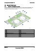
Intel® Compute Module MFS2600KI TPS 2.2 Product Overview Compute Module Layout 2.2.1 Connector and Component Locations The following figure shows the board layout of the Intel® Compute Module MFS2600KI. Each connector and major component is identified by a number or letter. A description of each identified item is provided below the figure.
Product Overview 2.2.3 Intel® Compute Module MFS2600KI TPS External I/O Connector Locations The following drawing shows the layout of the external I/O components for the Intel® Compute Module MFS2600KI. A USB ports 0 and 1 G NIC 1 LED B USB ports 2 and 3 H Hard Drive Activity LED C Video I ID LED D I/O Mezzanine NIC 4 LED J Power button E I/O Mezzanine NIC 3 LED K Power and Fault LEDs F NIC 2 LED ® Figure 2. Intel Compute Module MFS2600KI Front Panel Layout 4 Revision 1.
Intel® Compute Module MFS2600KI TPS 3. Functional Architecture Functional Architecture The architecture of the Intel® Compute Module MFS2600KI is developed around the integrated features and functions of the Intel® Xeon® processor E5-2600 product family the Intel® C602-J chipset, the Intel® Ethernet Controller I350 GbE controller chip and the Baseboard Management Controller.
Functional Architecture 3.1.1.1 Intel® Compute Module MFS2600KI TPS Processor Socket Assembly Each processor socket of the server board is pre-assembled with an Independent Latching Mechanism (ILM) and Back Plate which allow for secure placement of the processor and processor heat to the server board. The illustration below identifies each sub-assembly component. Heat Sink Server Board Independent Latching Mechanism (ILM) Back Plate Figure 4. Processor Socket Assembly 3.1.1.
Intel® Compute Module MFS2600KI TPS Functional Architecture Processors which have different Intel® Quickpath (QPI) Link Frequencies may operate together if they are otherwise compatible and if a common link frequency can be selected. The common link frequency would be the highest link frequency that all installed processors can achieve. Processor stepping within a common processor family can be mixed as long as it is listed in the processor specification updates published by Intel Corporation. 3.1.
Functional Architecture Intel® Compute Module MFS2600KI TPS Table 2. Mixed Processor Configurations Error Processor family not Identical Severity Fatal Processor model not Identical Fatal Processor cores/threads not identical Fatal System Action The BIOS detects the error condition and responds as follows: Logs the POST Error Code into the System Event Log (SEL). Alerts the BMC to set the System Status LED to steady Amber.
Intel® Compute Module MFS2600KI TPS Error ® Processor Intel QuickPath Interconnect link frequencies not identical Functional Architecture Severity Fatal System Action The BIOS detects the QPI link frequencies and responds as follows: Adjusts all QPI interconnect link frequencies to highest common frequency. No error is generated – this is not an error condition. Continues to boot the system successfully.
Functional Architecture 3.2.1 Intel® Compute Module MFS2600KI TPS Intel® Trusted Execution Technology (Intel® TXT) Intel® 64 Architecture Intel® Streaming SIMD Extensions 4.1 (Intel® SSE4.1) Intel® Streaming SIMD Extensions 4.2 (Intel® SSE4.
Intel® Compute Module MFS2600KI TPS Functional Architecture ® Table 3. Intel Compute Module MFS2600KI PCIe Bus Segment Characteristics CPU# 3.3.
Functional Architecture 3.4.1.1 Intel® Compute Module MFS2600KI TPS Independent channel mode or lockstep mode Data burst length of eight cycles for all memory organization modes Memory DDR3 data transfer rates of 800, 1066, 1333, and 1600 MT/s 64-bit wide channels plus 8-bits of ECC support for each channel DDR3 standard I/O Voltage of 1.5 V and DDR3 Low Voltage of 1.
Intel® Compute Module MFS2600KI TPS Functional Architecture The silk screened DIMM slot identifiers on the board provide information about the channel, and therefore the processor to which they belong. For example, DIMM_A1 is the first slot on Channel A on processor 1; DIMM_E1 is the first DIMM socket on Channel E on processor 2. The memory slots associated with a given processor are unavailable if the corresponding processor socket is not populated.
Functional Architecture Intel® Compute Module MFS2600KI TPS Table 5. RDIMM Support Guidelines (Preliminary. Subject to Change) Ranks Per DIMM and Data Width Memory Capacity Per DIMM1 Speed (MT/s) and Voltage Validated by Slot per Channel (SPC) and DIMM Per Channel (DPC)2 1 Slot per Channel 2 Slots per Channel 1DPC SRx8 1GB 2GB 4GB DRx8 2GB 4GB 8GB SRx4 2GB 4GB 8GB DRx4 4GB 8GB 16GB QRx4 8GB 16GB 32GB QRx8 4GB 8GB 16GB 1.
Intel® Compute Module MFS2600KI TPS Functional Architecture Supported and Validated 3.4.2 Publishing Compute Module Memory The BIOS displays the “Total Memory” of the compute module during POST if Display Logo is disabled in the BIOS setup. This is the total size of memory discovered by the BIOS during POST, and is the sum of the individual sizes of installed DDR3 DIMMs in the system. The BIOS displays the “Effective Memory” of the compute module in the BIOS setup.
Functional Architecture Intel® Compute Module MFS2600KI TPS Rank Sparing Mode is only possible when all channels that are populated with memory meet the requirement of having at least two SR or DR DIMM installed, or at least one QR DIMM installed, on each populated channel. Lockstep or Mirroring Modes require that for any channel pair that is populated with memory, the memory population on both channels of the pair must be identically sized.
Intel® Compute Module MFS2600KI TPS Functional Architecture Table 9. DDR3 UDIMM Population within a Channel Configuration Number 1 Speed 1N or 2N DIMM 2 DIMM 1 (Blue Slot) Empty Single-rank DDR3-1333, and 1066 1N 2 DDR3-1333, and 1066 1N Empty Dual-rank 3 DDR3-1333, and 1066 2N Single-rank Single-rank 4 DDR3-1333, and 1066 2N Single-rank Dual-rank 5 DDR3-1333, and 1066 2N Dual-rank Dual-rank Table 10.
Functional Architecture Intel® Compute Module MFS2600KI TPS Figure 6. DIMM Slot Order 3.4.3.1 Memory Subsystem Nomenclature The nomenclature for DIMM sockets implemented on the Intel® Compute Module MFS2600KI is detailed in the following table. ® Table 11.
Intel® Compute Module MFS2600KI TPS 3.4.3.2 Functional Architecture Publishing System Memory The BIOS displays the “Total Memory” of the system during POST if Quite Boot is disabled in the BIOS setup. This is the total size of memory discovered by the BIOS during POST, and is the sum of the individual sizes of installed DDR3 DIMMs in the system. The BIOS displays the “Effective Memory” of the system in the BIOS setup.
Functional Architecture 3.4.4.4 Intel® Compute Module MFS2600KI TPS Mirrored Channel Mode In Mirrored Channel Mode, the memory contents are mirrored between Channel 0 and Channel 2 and also between Channel 1 and Channel 3. As a result of the mirroring, the total physical memory available to the system is half of what is populated. Mirrored Channel Mode requires that Channel 0 and Channel 2, and Channel 1 and Channel 3 must be populated identically with regards to size and organization.
Intel® Compute Module MFS2600KI TPS Functional Architecture JTAG Boundary-Scan KVM/Serial Over LAN (SOL) Function 3.5.1 Digital Media Interface (DMI) Digital Media Interface (DMI) is the chip-to-chip connection between the processor and Intel® C602-J chipset. This high-speed interface integrates advanced priority-based servicing allowing for concurrent traffic and true isochronous transfer capabilities.
Functional Architecture 3.5.7 Intel® Compute Module MFS2600KI TPS Universal Serial Bus (USB) Controllers ® The Intel C602-J chipset has up to two Enhanced Host Controller Interface (EHCI) host controllers that support USB high-speed signaling. High-speed USB 2.0 allows data transfers up to 480 Mb/s which is 40 times faster than full-speed USB. The Intel® C602-J chipset supports up to fourteen USB 2.0 ports. All fourteen ports are high-speed, full-speed, and low-speed capable.
Intel® Compute Module MFS2600KI TPS Functional Architecture Two Fully Functional Serial Ports, compatible with the 16C550 Serial IRQ Support Up to 16 Shared direct GPIO’s Serial GPIO support for 80 general purpose inputs and 80 general purpose outputs available for host processor Programmable Wake-up Event Support Plug and Play Register Set Power Supply Control Host SPI bridge for system BIOS support 3.6.1.
Functional Architecture Intel® Compute Module MFS2600KI TPS ** Video resolutions at 1600x1200 and higher are only supported through the external video connector located on the rear I/O section of the server board. Utilizing the optional front panel video connector may result in lower video resolutions. The server board provides two video interfaces. The primary video interface is accessed using a standard 15-pin VGA connector found on the back edge of the server board.
Intel® Compute Module MFS2600KI TPS Interrupt controller Multiple SPI flash interfaces NAND/Memory interface Sixteen mailbox registers for communication between the BMC and host LPC ROM interface BMC watchdog timer capability SD/MMC card controller with DMA support LED support with programmable blink rate controls on GPIOs Port 80h snooping capability Secondary Service Processor (SSP), which provides the HW capability of off-loading time critical processing tasks from the main ARM core.
Functional Architecture Intel® Compute Module MFS2600KI TPS Intel® I350 NIC will be used in conjunction with the Emulex* Pilot-III Management Controller for out of band Management traffic. The BMC will communicate with Intel® I350 NIC over a NC-SI interface (RMII physical). Intel® I350 NIC will be on standby power so that the BMC can send management traffic over the NC-SI interface to the network during sleep state S5. 3.
Intel® Compute Module MFS2600KI TPS System Security 4. System Security 4.1 BIOS Password Protection The BIOS uses passwords to prevent unauthorized tampering with the server setup. Passwords can restrict entry to the BIOS Setup, restrict use of the Boot Popup menu, and suppress automatic USB device reordering. There is also an option to require a Power On password entry in order to boot the system.
System Security Intel® Compute Module MFS2600KI TPS prompts for a password, and can only be used with the Administrator password. Also, when a User password is defined, it suppresses the USB Reordering that occurs, if enabled, when a new USB boot device is attached to the system. A User is restricted from booting in anything other than the Boot Order defined in the Setup by an Administrator.
Intel® Compute Module MFS2600KI TPS System Security Verifies operator physical presence. Confirms and executes operating system TPM administrative command requests. Provides BIOS Setup options to change TPM security states and to clear TPM ownership. For additional details, refer to the TCG PC Client Specific Implementation Specification, the TCG PC Client Specific Physical Presence Interface Specification, and the Microsoft BitLocker* Requirement documents. 4.2.
System Security 4.3 Intel® Compute Module MFS2600KI TPS Intel® Trusted Execution Technology The Intel® Xeon® Processor E5-2600 support Intel® Trusted Execution Technology (Intel® TXT), which is a robust security environment. Designed to help protect against software-based attacks, Intel® Trusted Execution Technology integrates new security features and capabilities into the processor, chipset and other platform components.
Intel® Compute Module MFS2600KI TPS Connector/Header Locations and Pin-outs 5. Connector/Header Locations and Pin-outs 5.1 Board Connector Information The following section provides detailed information regarding all connectors, headers, and jumpers on the compute module. The following table lists all connector types available on the board and the corresponding reference designators printed on the silkscreen. Table 15. Board Connector Matrix 5.
Connector/Header Locations and Pin-outs 5.3 5.3.1 Intel® Compute Module MFS2600KI TPS I/O Connector Pin-out Definition VGA Connector The following table details the pin-out definition of the VGA connector (J2K1). Table 17. VGA Connector Pin-out (J2K1) Pin 5.3.
Intel® Compute Module MFS2600KI TPS Connector/Header Locations and Pin-outs Table 18.
Connector/Header Locations and Pin-outs Intel® Compute Module MFS2600KI TPS GND Signal Name 89 Pin Signal Name PCIe_1_D_TXP 90 Pin GND 91 PCIe_1_D_TXN 92 PCIe_1_D_RXP 93 GND 94 PCIe_1_D_RXN 95 GND 96 GND 97 Mezz_Present 98 GND 99 Reset_N 100 Clk0_100M_PCIE_P 101 GND 102 Clk0_100M_PCIE_N 103 GND 104 GND 105 Rsvd 106 GND 107 Rsvd 108 Rsvd 109 GND 110 Rsvd 111 Rsvd 112 Rsvd 113 Rsvd 114 P12V 115 P12V 116 P12V 117 P12V 118 P12V 119 P12V 120 Tab
Intel® Compute Module MFS2600KI TPS Connector/Header Locations and Pin-outs Signal Name PCIe_1_C_TXN Signal Description PCIe TX- of Lane C Link 1 Purpose Host connect 84 Connector Location PCIe_1_C_RXP PCIe RX+ of Lane C Link 1 Host connect 85 PCIe_1_C_RXN PCIe RX- of Lane C Link 1 Host connect 87 PCIe_1_D_TXP PCIe TX+ of Lane D Link 1 Host connect 90 PCIe_1_D_TXN PCIe TX- of Lane D Link 1 Host connect 92 PCIe_1_D_RXP PCIe RX+ of Lane D Link 1 Host connect 93 PCIe_1_D_RXN PCIe RX
Connector/Header Locations and Pin-outs Intel® Compute Module MFS2600KI TPS Table 20.
Intel® Compute Module MFS2600KI TPS Connector/Header Locations and Pin-outs Pin B4 Signal Name XE_P1_B_TXP Pin F4 Signal Name 12V (BL_PWR_ON) Pin J4 GND B5 XE_P1_C_RXN F5 GND J5 reserved B6 XE_P1_C_TXP F6 XE_P2_B_TXN J6 GND B7 XE_P1_D_RXN F7 GND J7 reserved B8 XE_P1_D_TXP F8 XE_P2_A_TXN J8 GND C1 GND G1 SAS_P1_RXP K1 SMB_SDA_A C2 XE_P1_A_TXN G2 GND K2 FM_BL_SLOT_ID0 C3 GND G3 XE_P2_C_RXP K3 FM_BL_SLOT_ID3 C4 XE_P1_B_TXN G4 GND K4 FM_BL_SLOT_ID4 C5 GND
Connector/Header Locations and Pin-outs Intel® Compute Module MFS2600KI TPS Table 23. External USB Connector Pin-out 5.3.6 Pin 1 +5V Signal Name USB_PWR Description 2 USB_N Differential data line paired with DATAH0 3 USB_P (Differential data line paired with DATAL0 4 GND Ground Low Profile eUSB SSD Support The system provides support for a low profile eUSB SSD storage device through a 2mm 2x5-pin connector (J1K1). The pin-out of the connector is detailed in the following table. Table 24.
Intel® Compute Module MFS2600KI TPS 6. Jumper Block Settings Jumper Block Settings The compute module has several 3-pin jumper blocks that can be used to configure, protect, or recover specific features of the server board. Pin 1 on each jumper block is denoted by an “*” or “▼”. Figure 9. Recovery Jumper Blocks Revision 1.
Jumper Block Settings Intel® Compute Module MFS2600KI TPS Table 25. Recovery Jumpers Jumper Name J1F3: BMC Force Update J1F4: BIOS J1F5: ME Force J1F8: CMOS Clear J1F9: Password 6.1 Pins What happens at system reset … 1-2 BMC Firmware Force Update Mode – Disabled (Default) 2-3 BMC Firmware Force Update Mode – Enabled 1-2 R e2-3 c o v e r These pins should have a jumper in place for normal operation.
Intel® Compute Module MFS2600KI TPS Jumper Block Settings Password and/or CMOS are now cleared and can be reset by going into the BIOS setup. 6.2 Integrated BMC Force Update Procedure When performing a standard Integrated BMC firmware update procedure, the update utility places the Integrated BMC into an update mode, allowing the firmware to load safely onto the flash device.
Jumper Block Settings Intel® Compute Module MFS2600KI TPS 1. Power down and remove the compute module from chassis. 2. Open the compute module enclosure 3. Move jumper from the default operating position (covering pins 1 and 2) to the enabled position (covering pins 2 and 3). 4. Close the compute module enclosure. 5. Reinsert the compute module and power up. 6. Perform the ME firmware update procedure as documented in the README.
Intel® Compute Module MFS2600KI TPS Product Regulatory Requirements 7. Product Regulatory Requirements 7.1 Product Regulatory Requirements The Intel® Compute Module MFS2600KI is evaluated as part of the Intel® Modular Server System MFSYS25V2, which requires meeting all applicable system component regulatory requirements. Refer to the Intel® Modular Server System Technical Product Specification for a complete listing of all system and component regulatory requirements. 7.
Appendix A: Integration and Usage Tips Intel® Compute Module MFS2600KI TPS Appendix A: Integration and Usage Tips When two processors are installed, both must be of identical revision, core voltage, and bus/core speed. Mixed processor steppings are supported as long as they are listed in the processor specification updates published by Intel Corporation. However, the stepping of one processor cannot be greater than one stepping back of the other.
Intel® Compute Module MFS2600KI TPS Appendix B: POST Code Diagnostic LED Decoder Appendix B: POST Code Diagnostic LED Decoder During the system boot process, the BIOS executes a number of platform configuration processes, each of which is assigned a specific hex POST code number. As each configuration routine is started, the BIOS displays the POST code to the POST Code Diagnostic LEDs on the back edge of the server board.
Appendix B: POST Code Diagnostic LED Decoder Intel® Compute Module MFS2600KI TPS Upper nibble bits = 1010b = Ah; Lower nibble bits = 1100b = Ch; the two are concatenated as ACh The following table provides a list of all POST progress codes. Table 27.
Intel® Compute Module MFS2600KI TPS Checkpoint Appendix B: POST Code Diagnostic LED Decoder Diagnostic LED Decoder 1 = LED On, 0 = LED Off Upper Nibble Lower Nibble MSB LSB 8h 4h 2h 1h 8h 4h 2h 1h #7 #6 #5 #4 #3 #2 #1 #0 1 0 0 1 0 1 0 1 1 0 0 1 0 1 1 0 1 0 0 1 0 1 1 1 1 0 0 1 1 0 0 0 1 0 0 1 1 0 0 1 1 0 0 1 1 0 1 0 1 0 0 1 1 0 1 1 1 0 0 1 1 1 0 0 1 0 0 1 1 1 0 1 1 0 1 0 0 0 0 1 1 0 1 0 0 0 1 0 1 0 1 0 0 0 1 1 1 0 1 0 0 1 0 0 1 0 1 0 0 1 0 1 1 0 1 0 0 1 1 0 1 0 1 0 0 1 1 1 1 0 1 0 1 0 0 0 1 0 1 0 1 0 0 1 1
Appendix B: POST Code Diagnostic LED Decoder Intel® Compute Module MFS2600KI TPS The MRC Progress Codes are displays to the Diagnostic LEDs that show the execution point in the MRC operational path at each step. Table 28.
Intel® Compute Module MFS2600KI TPS Appendix B: POST Code Diagnostic LED Decoder Diagnostic LED Decoder 1 = LED On, 0 = LED Off Upper Nibble Checkpoint Lower Nibble Description MSB LED EBh EDh EFh Revision 1.
Appendix C: POST Error Code Intel® Compute Module MFS2600KI TPS Appendix C: POST Error Code Most error conditions encountered during POST are reported using POST Error Codes. These codes represent specific failures, warnings, or informational messages that are identified with particular hardware units. These POST Error Codes may be displayed in the Error Manager display screen, and are always automatically logged to the System Event Log (SEL).
Intel® Compute Module MFS2600KI TPS Appendix C: POST Error Code Error Code 8163 Error Message Processor 04 unable to apply microcode update Response Major 8170 Processor 01 failed Self Test (BIST) Major 8171 Processor 02 failed Self Test (BIST) Major 8172 Processor 03 failed Self Test (BIST) Major 8173 Processor 04 failed Self Test (BIST) Major 8180 Processor 01 microcode update not found Minor 8181 Processor 02 microcode update not found Minor 8182 Processor 03 microcode update not
Appendix C: POST Error Code Intel® Compute Module MFS2600KI TPS Error Code 8539 DIMM_I2 failed test/initialization Response Major 853A DIMM_I3 failed test/initialization Major 853B DIMM_J1 failed test/initialization Major 853C DIMM_J2 failed test/initialization Major 853D DIMM_J3 failed test/initialization Major 853E DIMM_K1 failed test/initialization Major 853F (Go to 85C0) DIMM_K2 failed test/initialization Major 8540 DIMM_A1 disabled Major 8541 DIMM_A2 disabled Major 8542 DI
Intel® Compute Module MFS2600KI TPS Appendix C: POST Error Code Error Code 8564 Error Message DIMM_B2 encountered a Serial Presence Detection (SPD) failure Response Major 8565 DIMM_B3 encountered a Serial Presence Detection (SPD) failure Major 8566 DIMM_C1 encountered a Serial Presence Detection (SPD) failure Major 8567 DIMM_C2 encountered a Serial Presence Detection (SPD) failure Major 8568 DIMM_C3 encountered a Serial Presence Detection (SPD) failure Major 8569 DIMM_D1 encountered a Seri
Appendix C: POST Error Code Intel® Compute Module MFS2600KI TPS Error Code 85D0 DIMM_K3 disabled Response Major 85D1 DIMM_L1 disabled Major 85D2 DIMM_L2 disabled Major 85D3 DIMM_L3 disabled Major 85D4 DIMM_M1 disabled Major 85D5 DIMM_M2 disabled Major 85D6 DIMM_M3 disabled Major 85D7 DIMM_N1 disabled Major 85D8 DIMM_N2 disabled Major 85D9 DIMM_N3 disabled Major 85DA DIMM_O1 disabled Major 85DB DIMM_O2 disabled Major 85DC DIMM_O3 disabled Major 85DD DIMM_P1 disabled
Intel® Compute Module MFS2600KI TPS Appendix C: POST Error Code The following table lists the POST error beep codes. Prior to system video initialization, the BIOS uses these beep codes to inform users on error conditions. The beep code is followed by a user-visible code on the POST Progress LEDs Table 31.
Appendix D: Supported Intel® Modular Server System Intel® Compute Module MFS2600KI TPS Appendix D: Supported Intel® Modular Server System The Intel® Compute Module MFS5520VI is supported in the following chassis: Intel® Modular Server System MFSYS25V2 This section provides a high-level pictorial overview of the Intel® Modular Server System MFSYS25V2. For more details, refer to the Intel® Modular Server System Technical Product Specification (TPS).
Intel® Compute Module MFS2600KI TPS Glossary Glossary This appendix contains important terms used in the preceding chapters. For ease of use, numeric entries are listed first (for example, “82460GX”) followed by alpha entries (for example, “AGP 4x”). Acronyms are followed by non-acronyms.
Glossary Intel® Compute Module MFS2600KI TPS Term Definition IFB I/O and Firmware Bridge INTR Interrupt IP Internet Protocol IPMB Intelligent Platform Management Bus IPMI Intelligent Platform Management Interface IR Infrared ITP In-Target Probe KB 1024 bytes KCS Keyboard Controller Style LAN Local Area Network LCD Liquid Crystal Display LED Light Emitting Diode LPC Low Pin Count LUN Logical Unit Number MAC Media Access Control MB 1024KB MCH Memory Controller Hub MD2 Me
Intel® Compute Module MFS2600KI TPS Glossary Term SMBus* System Management Bus SMI Server Management Interrupt (SMI is the highest priority non-maskable interrupt) SMM Server Management Mode SMS Server Management Software SNMP Simple Network Management Protocol TBD To Be Determined TIM Thermal Interface Material UART Universal Asynchronous Receiver/Transmitter UDP User Datagram Protocol UHCI Universal Host Controller Interface UTC Universal time coordinate VID Voltage Identification
Reference Documents Intel® Compute Module MFS2600KI TPS Reference Documents For additional information, refer to the Intel® Modular Server System Technical Product Specification. 60 Intel Confidential Intel order number: G51989-002 Revision 1.