Intel® Core™ i7 Processor Family for LGA2011 Socket Datasheet – Volume 1 of 2 Supporting Desktop Intel® Core™ i7-4960X Extreme Edition Processor Series for the LGA2011 Socket Supporting Desktop Intel® Core™ i7-49xx and i7-48xx Processor Series for the LGA2011 Socket September 2013 329366-001
INFORMATION IN THIS DOCUMENT IS PROVIDED IN CONNECTION WITH INTEL PRODUCTS. NO LICENSE, EXPRESS OR IMPLIED, BY ESTOPPEL OR OTHERWISE, TO ANY INTELLECTUAL PROPERTY RIGHTS IS GRANTED BY THIS DOCUMENT.
Table of Contents 1 Introduction ..............................................................................................................8 1.1 Processor Feature Details .....................................................................................9 1.2 Supported Technologies ..................................................................................... 10 1.3 Interfaces ........................................................................................................ 10 1.3.
.2 4.3 4.4 Processor Core / Package Power Management ...................................................... 4.2.1 Enhanced Intel® SpeedStep® Technology ................................................. 4.2.2 Low-Power Idle States ............................................................................ 4.2.3 Requesting Low-Power Idle States ........................................................... 4.2.4 Core C-states ..................................................................................
Figures 1-1 1-2 2-1 2-2 4-1 4-2 4-3 7-1 7-2 7-3 Processor Platform Block Diagram Example.............................................................9 PCI Express* Lane Partitioning and Direct Media Interface Gen 2 (DMI2) .................. 12 PCI Express* Layering Diagram........................................................................... 19 Packet Flow through the Layers ...........................................................................
7-10 7-11 7-12 7-13 7-14 7-15 7-16 7-17 7-18 7-19 7-20 8-1 8-2 6 Voltage Specifications........................................................................................ Current Specifications........................................................................................ VCC Overshoot Specifications .............................................................................. DDR3 and DDR3L Signal DC Specifications ...........................................................
Revision History Revision Number 001 Description • Initial release Date September 2013 § Datasheet 7
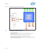
Introduction 1 Introduction The Intel® Core™ i7 processor family for LGA2011 socket are the next generation of 64-bit, multi-core desktop processors built on 22-nanometer process technology. Based on the low-power/high-performance Intel® Core™ i7 processor micro-architecture, the processor is designed for a two-chip platform instead of to the traditional three-chip platforms (processor, Memory Controller Hub, and Platform Controller Hub).
Introduction Figure 1-1. Processor Platform Block Diagram Example 1.1 Processor Feature Details • Up to 6 execution cores • Each core supports two threads (Intel® Hyper-Threading Technology), up to 12 threads per socket • 32KB instruction and 32-KB data first-level cache (L1) for each core • 256KB shared instruction/data mid-level (L2) cache for each core • Up to 15MB last level cache (LLC): up to 2.
Introduction 1.2 Supported Technologies • Intel® Virtualization Technology (Intel® VT) • Intel® Virtualization Technology (Intel® VT) for Directed I/O (Intel® VT-d) • Intel® Virtualization Technology (Intel® VT) Processor Extensions • Intel® 64 Architecture • Intel® Streaming SIMD Extensions 4.1 (Intel® SSE4.1) • Intel® Streaming SIMD Extensions 4.2 (Intel® SSE4.
Introduction 1.3.2 PCI Express* • The PCI Express* port(s) are fully-compliant with the PCI Express* Base Specification, Revision 3.0 (PCIe 3.0) • Support for PCI Express* 3.0 (8.0 GT/s), 2.0 (5.0 GT/s), and 1.0 (2.5 GT/s) • Up to 40 lanes of PCI Express* interconnect for general purpose PCI Express* devices at PCIe* 3.0 speeds that are configurable for up to 10 independent ports • 4 lanes of PCI Express* at PCIe* 2.
Introduction Figure 1-2. PCI Express* Lane Partitioning and Direct Media Interface Gen 2 (DMI2) 1.3.3 Direct Media Interface Gen 2 (DMI2) • Serves as the chip-to-chip interface to the PCH • The DMI2 port supports x4 link width and only operates in a x4 mode when in DMI2 • Operates at PCI Express* 1.0 or 2.0 speeds • Transparent to software • Processor and peer-to-peer writes and reads with 64-bit address support • APIC and Message Signaled Interrupt (MSI) support.
Introduction 1.3.4 Platform Environment Control Interface (PECI) The PECI is a one-wire interface that provides a communication channel between a PECI client (the processor) and a PECI master (the PCH). Refer to the Processor Thermal Mechanical Specifications and Design Guide for additional details on PECI services available in the processor (Refer to the Related Documents section).
Introduction 1.6 Package Summary The processor socket type is noted as LGA2011. The processor package is a 52.5 x 45 mm FC-LGA package (LGA2011). Refer to the Processor Thermal Mechanical Specification and Design Guide (see Related Documents section) for the package mechanical specifications. 1.7 Terminology Table 1-1.
Introduction Table 1-1. Terminology (Sheet 2 of 3) Term Description ® Datasheet Intel® VT-d Intel Virtualization Technology (Intel® VT) for Directed I/O. Intel VT-d is a hardware assist, under system software (Virtual Machine Manager or operating system) control, for enabling I/O device virtualization. Intel VT-d also brings robust security by providing protection from errant DMAs by using DMA remapping, a key feature of Intel VT-d.
Introduction Table 1-1. Terminology (Sheet 3 of 3) Term Description TSOD Thermal Sensor on DIMM UDIMM Unbuffered Dual In-line Module Uncore Unit Interval The portion of the processor comprising the shared cache, IMC, HA, PCU, and UBox. Signaling convention that is binary and unidirectional. In this binary signaling, one bit is sent for every edge of the forwarded clock, whether it be a rising edge or a falling edge. If a number of edges are collected at instances t1, t2, tn,....
Introduction Table 1-3. Public Specifications Document Document Number / Location Advanced Configuration and Power Interface Specification 3.0 http://www.acpi.info PCI Local Bus Specification 3.0 http://www.pcisig.com/specifications PCI Express Base Specification - Revision 2.1 and 1.1 PCI Express Base Specification - Revision 3.0 http://www.pcisig.com System Management Bus (SMBus) Specification, Revision 2.0 http://smbus.org/ DDR3 SDRAM Specification http://www.jedec.
Interfaces 2 Interfaces This chapter describes the functional behaviors supported by the processor. Topics covered include: • System Memory Interface • PCI Express* Interface • Direct Media Interface 2 (DMI2) / PCI Express* Interface • Platform Environment Control Interface (PECI) 2.1 System Memory Interface 2.1.1 System Memory Technology Support The Integrated Memory Controller (IMC) supports DDR3 protocols with four independent 64-bit memory channels and supports 1 unbuffered DIMM per channel. 2.1.
Interfaces 2.2 PCI Express* Interface This section describes the PCI Express* 3.0 interface capabilities of the processor. See the PCI Express* Base Specification for details of PCI Express* 3.0. 2.2.1 PCI Express* Architecture Compatibility with the PCI addressing model is maintained to ensure that all existing applications and drivers operate unchanged. The PCI Express* configuration uses standard mechanisms as defined in the PCI Plug-and-Play specification.
Interfaces 2.2.1.1 Transaction Layer The upper layer of the PCI Express* architecture is the Transaction Layer. The Transaction Layer's primary responsibility is the assembly and disassembly of Transaction Layer Packets (TLPs). TLPs are used to communicate transactions, such as read and write, as well as certain types of events. The Transaction Layer also manages flow control of TLPs. 2.2.1.
Interfaces 2.3 Direct Media Interface 2 (DMI2) / PCI Express* Interface Direct Media Interface 2 (DMI2) connects the processor to the Platform Controller Hub (PCH). DMI2 is similar to a four-lane PCI Express* supporting a speed of 5 GT/s per lane. Refer to Section 6.3 for additional details. Note: Only DMI2 x4 configuration is supported. 2.3.1 DMI2 Error Flow DMI2 can only generate SERR in response to errors, never SCI, SMI, MSI, PCI INT, or GPE.
Technologies 3 Technologies This chapter covers the following technologies: • Intel® Virtualization Technology (Intel® VT) • Security Technologies • Intel® Hyper-Threading Technology (Intel® HT Technology) • Intel® Turbo Boost Technology • Enhanced Intel® SpeedStep® Technology • Intel® Advanced Vector Extensions (Intel® AVX) 3.1 Intel® Virtualization Technology (Intel® VT) Intel® Virtualization Technology (Intel® VT) makes a single system appear as multiple independent systems to software.
Technologies 3.1.2 Intel® VT-x Features The processor core supports the following Intel VT-x features: • Extended Page Tables (EPT) — hardware assisted page table virtualization. — eliminates VM exits from guest operating system to the VMM for shadow pagetable maintenance. • Virtual Processor IDs (VPID) — Ability to assign a VM ID to tag processor core hardware structures (such as, TLBs).
Technologies 3.1.3.
Technologies 3.2 Security Technologies 3.2.1 Intel® Advanced Encryption Standard New Instructions (Intel® AES-NI) Instructions These instructions enable fast and secure data encryption and decryption, using the Advanced Encryption Standard (Intel AES-NI) which is defined by FIPS Publication number 197. Since Intel AES-NI is the dominant block cipher, and it is deployed in various protocols, the new instructions will be valuable for a wide range of applications.
Technologies 3.4 Intel® Turbo Boost Technology Intel Turbo Boost Technology is a feature that allows the processor to opportunistically and automatically run faster than its rated operating frequency if it is operating below power, temperature, and current limits. The result is increased performance in multithreaded and single threaded workloads. It should be enabled in the BIOS for the processor to operate with maximum performance. 3.4.
Technologies 3.6 Intel® Advanced Vector Extensions (Intel® AVX) Intel Advanced Vector Extensions (Intel AVX) is a new 256-bit vector SIMD extension of Intel Architecture. The introduction of Intel AVX started with the 2nd Generation Intel® Core™ processor family. Intel AVX accelerates the trend of parallel computation in general purpose applications like image, video and audio processing, engineering applications (such as 3D modeling and analysis), scientific simulation, and financial analysts.
Technologies • Compatibility – Intel AVX is backward compatible with previous ISA extensions including Intel SSE4: — Existing Intel SSE applications/library can: • Run unmodified and benefit from processor enhancements • Recompile existing Intel® SSE intrinsic using compilers that generate Intel AVX code • Inter-operate with library ported to Intel AVX — Applications compiled with Intel AVX can inter-operate with existing Intel SSE libraries.
Power Management 4 Power Management This chapter provides information on the following power management topics: • Advanced Configuration and Power Interface (ACPI) States Supported • Processor Core / Package Power Management • System Memory Power Management • Direct Media Interface 2 (DMI2) / PCI Express* Power Management 4.1 Advanced Configuration and Power Interface (ACPI) States Supported The ACPI states supported by the processor are described in this section. 4.1.1 System States Table 4-1.
Power Management Table 4-2.
Power Management 4.1.3 Integrated Memory Controller (IMC) States Table 4-4. System Memory Power States State Description Power Up/Normal Operation CKE asserted. Active Mode, highest power consumption. CKE Power Down Opportunistic, per rank control after idle time: • Active Power Down (APD) (default mode) — CKE de-asserted. Power savings in this mode, relative to active idle state is about 55% of the memory power. Exiting this mode takes 3 – 5 DCLK cycles.
Power Management 4.1.5 G, S, and C State Combinations Table 4-6. G, S and C State Combinations 4.
Power Management 4.2.2 Low-Power Idle States When the processor is idle, low-power idle states (C-states) are used to save power. More power savings actions are taken for numerically higher C-States. However, higher C-states have longer exit and entry latencies. Resolution of C-states occurs at the thread, processor core, and processor package level. Thread level C-states are available if Intel Hyper-Threading Technology is enabled.
Power Management Table 4-7. Coordination of Thread Power States at the Core Level Processor Core C-State Thread 0 Thread 1 C0 C1 C3 C6 C7 C0 C0 C0 C0 C0 C0 C1 C0 C11 C11 C11 C11 C3 C0 C11 C3 C3 C3 C6 C0 C11 C3 C6 C6 C7 C0 C11 C3 C6 C7 Note: 1. If enabled, the core C-state will be C1E if all actives cores have also resolved a core C1 state or higher. 4.2.
Power Management 4.2.4 Core C-states The following are general rules for all core C-states, unless specified otherwise: • A core C-state is determined by the lowest numerical thread state (such as, Thread 0 requests C1E while Thread 1 requests C3, resulting in a core C1E state). See Table 4-6. • A core transitions to C0 state when: — an interrupt occurs. — there is an access to the monitored address if the state was entered using an MWAIT instruction.
Power Management 4.2.4.6 Delayed Deep C-States The Delayed Deep C-states (DDCst) feature on this processor replaces the “C-state auto-demotion” scheme used in the previous processor generation. Deep C-states are defined as CC3 through CC7 (refer to Table 4-3 for supported deep C-states).
Power Management There is also a concept of Execution Allowed (EA). When EA status is 0, the cores in a socket are in C3 or a deeper state; a socket initiates a request to enter a coordinated package C-state. The coordination is across all sockets and the PCH. Table 4-9 shows an example of a dual-core processor package C-state resolution. Figure 4-3 summarizes package C-state transitions with package C2 as the interim between PC0 and PC1 prior to PC3 and PC6. Table 4-9.
Power Management 4.2.5.2 Package C1/C1E State No additional power reduction actions are taken in the package C1 state. However, if the C1E substate is enabled, the processor automatically transitions to the lowest supported core clock frequency, followed by a reduction in voltage. Autonomous power reduction actions that are based on idle timers, can trigger depending on the activity in the system. The package enters the C1 low-power state when: • At least one core is in the C1 state.
Power Management 4.2.5.5 Package C6 State A processor enters the package C6 low-power state when: • At least one core is in the C6 state. • The other cores are in a C6 or lower power state, and the processor has been granted permission by the platform. • L3 shared cache retains context and becomes inaccessible in this state.
Power Management 4.3.1 CKE Power-Down The CKE input land is used to enter and exit different power-down modes. The memory controller has a configurable activity timeout for each rank. When no reads are present to a given rank for the configured interval, the memory controller will transition the rank to power-down mode. The memory controller transitions the DRAM to power-down by de-asserting CKE and driving a NOP command.
Power Management 4.3.2.2 Self-Refresh Exit Self-refresh exit can be either a message from an external unit (PCU in most cases, but also possibly from any message-channel master) or as reaction for an incoming transaction. Here are the proper actions on self-refresh exit: • CK is enabled, and four CK cycles driven. • When proper skew between Address/Command and CK are established, assert CKE. • Issue NOPs for tXSRD cycles. • Issue ZQCL to each rank. • The global scheduler will be enabled to issue commands.
Thermal Management Specifications 5 Thermal Management Specifications The processor requires a thermal solution to maintain temperatures within operating limits. Any attempt to operate the processor outside these limits may result in permanent damage to the processor and potentially other components within the system. Maintaining the proper thermal environment is key to reliable, long-term system operation. A complete solution includes both component and system-level thermal management features.
Signal Descriptions 6 Signal Descriptions This chapter describes the processor signals. The signals are arranged in functional groups according to their associated interface or category. 6.1 System Memory Interface Signals Table 6-1. Memory Channel DDR0, DDR1, DDR2, DDR3 Signal Name Datasheet Description DDR{0/1/2/3}_BA[2:0] Bank Address: These signals define the bank which is the destination for the current Activate, Read, Write, or PRECHARGE command.
Signal Descriptions Table 6-2. Memory Channel Miscellaneous Signal Name Description DDR_RESET_C01_N DDR_RESET_C23_N System Memory Reset: Reset signal from processor to DRAM devices on the DIMMs. DDR_RESET_C01_N is used for memory channels 0 and 1 while DDR_RESET_C23_N is used for memory channels 2 and 3. DDR_SCL_C01 DDR_SCL_C23 SMBus clock for the dedicated interface to the serial presence detect (SPD) and thermal sensors (TSoD) on the DIMMs.
Signal Descriptions Table 6-4. PCI Express* Port 2 Signals (Sheet 2 of 2) Signal Name Table 6-5. Description PE2B_TX_DN[7:4] PE2B_TX_DP[7:4] PCIe Transmit Data Output PE2C_TX_DN[11:8] PE2C_TX_DP[11:8] PCIe Transmit Data Output PE2D_TX_DN[15:12] PE2D_TX_DP[15:12] PCIe Transmit Data Output PCI Express* Port 3 Signals Signal Name Table 6-6.
Signal Descriptions 6.3 Direct Media Interface Gen 2 (DMI2) / PCI Express* Port 0 Signals Table 6-7. DMI2 and PCI Express Port 0 Signals Signal Name Description DMI_RX_DN[3:0] DMI_RX_DP[3:0] DMI2 Receive Data Input DMI_TX_DP[3:0] DMI_TX_DN[3:0] DMI2 Transmit Data Output 6.4 Platform Environment Control Interface (PECI) Signal Table 6-8.
Signal Descriptions Table 6-10. Joint Test Action Group (JTAG) and Test Access Port (TAP) Signals (Sheet 2 of 2) Signal Name 6.7 Description TDO Test Data Out: This signal transfers serial test data out of the processor. TDO provides the serial output needed for JTAG specification support. TMS Test Mode Select: This signal is a JTAG specification support signal used by debug tools. TRST_N Test Reset: This signal resets the Test Access Port (TAP) logic.
Signal Descriptions Table 6-12. Processor Asynchronous Sideband Signals (Sheet 2 of 3) Signal Name PROCHOT_N PWRGOOD Description Processor Hot: PROCHOT_N will go active when the processor temperature monitoring sensor detects that the processor has reached its maximum safe operating temperature. This indicates that the processor Thermal Control Circuit has been activated, if enabled. This signal can also be driven to the processor to activate the Thermal Control Circuit.
Signal Descriptions Table 6-12. Processor Asynchronous Sideband Signals (Sheet 3 of 3) Signal Name Description TXT_AGENT Intel® Trusted Execution Technology (Intel® TXT) Agent: This is a strap signal: 0 = Default. The socket is not the Intel® TXT Agent. 1 = The socket is the Intel® TXT Agent. In non-Scalable dual-processor (DP) platforms, the legacy socket (identified by SOCKET_ID[1:0] = 00b) with Intel TXT Agent should always set the TXT_AGENT to 1b.
Signal Descriptions 6.9 Processor Power and Ground Supplies Table 6-14. Power and Ground Signals Signal Name VCC Description Variable power supply for the processor cores, lowest level caches (LLC), ring interface, and home agent. It is provided by a VRM/EVRD 12.0 compliant regulator for each processor socket. The output voltage of this supply is selected by the processor, using the serial voltage ID (SVID) bus. Note: VCC has a Vboot setting of 0.0 V and is not included in the PWRGOOD indication.
Electrical Specifications 7 Electrical Specifications This chapter covers the following topics: • Processor Signaling • Signal Group Summary • Power-On Configuration (POC) Options • Absolute Maximum and Minimum Ratings • DC Specifications 7.1 Processor Signaling The processor includes 2011 lands that use various signaling technologies. Signals are grouped by electrical characteristics and buffer type into various signal groups.
Electrical Specifications 7.1.4 Platform Environmental Control Interface (PECI) PECI is an Intel proprietary interface that provides a communication channel between Intel processors and chipset components to external system management logic and thermal monitoring devices. The processor contains a Digital Thermal Sensor (DTS) that reports a relative die temperature as an offset from Thermal Control Circuit (TCC) activation temperature.
Electrical Specifications Clock multiplying within the processor is provided by the internal phase locked loop (PLL) that requires a constant frequency BCLK{0/1}_DP, BCLK{0/1}_DN input, with exceptions for spread spectrum clocking. DC specifications for the BCLK{0/1}_DP, BCLK{0/1}_DN inputs are provided in Table 7-15. 7.1.5.1 PLL Power Supply An on-die PLL filter solution is implemented on the processor. Refer to Table 7-10 for DC specifications. 7.1.
Electrical Specifications Table 7-1. 7.1.8.2 Power and Ground Lands Power and Ground Lands Number of Lands Comments VCC 208 Each VCC land must be supplied with the voltage determined by the SVID Bus signals. Table 7-3 defines the voltage level associated with each core SVID pattern. VCC has a VBOOT setting of 0.0V. VCCPLL 3 Each VCCPLL land is connected to a 1.70 V supply to power the Phase Lock Loop (PLL) clock generation circuitry.
Electrical Specifications 7.1.8.3.1 Serial Voltage Identification (SVID) Commands The processor provides the ability to operate while transitioning to a new VID setting and its associated processor voltage rails (VCC, VSA, and VCCD). This is represented by a DC shift. It should be noted that a low-to-high or high-to-low voltage state change may result in as many VID transitions as necessary to reach the target voltage. Transitions above the maximum specified VID are not supported.
Electrical Specifications 7.1.8.3.5 SVID Power State Functions – SetPS The processor has three power state functions and these states will be set seamlessly with the SVID bus using the SetPS command. Based on the power state command, the SetPS commands send information to the VR controller to configure the VR to improve efficiency, especially at light loads.
Electrical Specifications 7.1.8.3.6 SVID Voltage Rail Addressing The processor addresses four different voltage rail control segments within VR12 (VCC, VCCD_01, VCCD_23, and VSA). The SVID data packet contains a 4-bit addressing code. Table 7-2. Serial Voltage Identification (SVID) Address Usage PWM Address (Hex) Processor 00 Vcc 01 Vsa 02 VCCD_01 03 +1 not used 04 VCCD_23 05 +1 not used Notes: 1.
Electrical Specifications Table 7-3. Hex VR12.0 Reference Code Voltage Identification (VID) Table (Sheet 2 of 2) VCC, VSA, VCCD Hex VCC, VSA, VCCD Hex VCC, VSA, VCCD Hex VCC, VSA, VCCD Hex VCC, VSA, VCCD Hex VCC, VSA, VCCD 1.50500 4D 0.63000 70 0.80500 93 0.98000 B6 1.15500 D9 1.33000 FC 4E 0.63500 71 0.81000 94 0.98500 B7 1.16000 DA 1.33500 FD 1.51000 4F 0.64000 72 0.81500 95 0.99000 B8 1.16500 DB 1.34000 FE 1.51500 50 0.64500 73 0.82000 96 0.
Electrical Specifications Table 7-5. Signal Groups (Sheet 1 of 3) Differential / Single Ended Buffer Type Signals1 DDR3 Reference Clocks2 Differential SSTL Output DDR{0/1/2/3}_CLK_D[N/P][3:0] DDR3 Command Signals2 Single ended SSTL Output DDR{0/1/2/3}_BA[2:0] DDR{0/1/2/3}_CAS_N DDR{0/1/2/3}_MA[15:00] DDR{0/1/2/3}_MA_PAR DDR{0/1/2/3}_RAS_N DDR{0/1/2/3}_WE_N CMOS1.5v Output DDR_RESET_C{01/23}_N DDR3 Control Signals2 CMOS1.
Electrical Specifications Table 7-5. Signal Groups (Sheet 2 of 3) Differential / Single Ended Signals1 Buffer Type PCI Express* Miscellaneous Signals Single ended Analog Input PE_RBIAS_SENSE Reference Input/Output PE_RBIAS PE_VREF_CAP DMI2/PCI Express* Signals Differential DMI2 Input DMI_RX_D[N/P][3:0] DMI2 Output DMI_TX_D[N/P][3:0] Platform Environmental Control Interface (PECI) Single ended PECI PECI System Reference Clock (BCLK{0/1}) Differential CMOS1.
Electrical Specifications Table 7-5. Signal Groups (Sheet 3 of 3) Differential / Single Ended Signals1 Buffer Type Power/Other Signals Power / Ground VCC, VTTA, VTTD, VCCD_01, VCCD_23,VCCPLL, VSA and VSS Sense Points VCC_SENSE VSS_VCC_SENSE VSS_VTTD_SENSE VTTD_SENSE VSA_SENSE VSS_VSA_SENSE Notes: 1. Refer to Chapter 6 for signal description details. 2. DDR{0/1/2/3} refers to DDR3 Channel 0, DDR3 Channel 1, DDR3 Channel 2 and DDR3 Channel 3. Table 7-6.
Electrical Specifications 7.4 Absolute Maximum and Minimum Ratings Table 7-8 specifies absolute maximum and minimum ratings. At conditions outside functional operation condition limits, but within absolute maximum and minimum ratings, neither functionality nor long-term reliability can be expected.
Electrical Specifications Table 7-9. Storage Condition Ratings (Sheet 2 of 2) Symbol Parameter Min Max Unit Tshort term storage The ambient storage temperature (in shipping media) for a short period of time. -20 85 °C RHsustained storage The maximum device storage relative humidity for a sustained period of time. Timesustained storage A prolonged or extended period of time; typically associated with sustained storage conditions Unopened bag, includes 6 months storage time by customer.
Electrical Specifications Table 7-10. Voltage Specifications (Sheet 2 of 2) Symbol Parameter VCCD (VCCD_01, VCCD_23) I/O Voltage for DDR3 (Standard Voltage) VTT (VTTA, Uncore Voltage VTTD) VSA_VID VSA Vsa VID Range System Agent Voltage Voltage Plane Min Typ Max Unit Notes1 VCCD 0.95*VCCD_TYP 1.5 1.05*VCCD_TYP V 11, 13, 14, 16, 17 VTT 0.957*VTT_TYP 1.00 1.043*VTT_TYP V 3, 5, 9, 12, 13 VSA 0.6 0.940 1.25 V 2, 3, 14, 15 VSA VSA_VID - 0.057 VSA_VID VSA_VID + 0.
Electrical Specifications Table 7-11.
Electrical Specifications 7.5.2 Die Voltage Validation Core voltage (VCC) overshoot events at the processor must meet the specifications in Table 7-12 when measured across the VCC_SENSE and VSS_VCC_SENSE lands. Overshoot events that are < 10 ns in duration may be ignored. These measurements of processor die level overshoot should be taken with a 100 MHz bandwidth limited oscilloscope. 7.5.2.
Electrical Specifications 7.5.3 Signal DC Specifications DC specifications are defined at the processor pads, unless otherwise noted. DC specifications are only valid while meeting specifications for case temperature, clock frequency, and input voltages. Care should be taken to read all notes associated with each specification. Table 7-13. DDR3 and DDR3L Signal DC Specifications (Sheet 1 of 2) Symbol IIL Parameter Input Leakage Current Min Typ Max Units Notes1 -1.4 — +1.
Electrical Specifications Table 7-13. DDR3 and DDR3L Signal DC Specifications (Sheet 2 of 2) Symbol Parameter Min Typ Max Units Notes1 DDR3 Miscellaneous Signals VIL Input Low Voltage DRAM_PWR_OK_C{01/23} — — 0.55*VCCD + 0.2 V 2, 3, 11, 13 VIH Input High Voltage DRAM_PWR_OK_C{01/23} 0.55*VCCD + 0.3 — — V 2, 4, 5, 11, 13 Notes: 1. Unless otherwise noted, all specifications in this table apply to all processor frequencies. 2. The voltage rail VCCD which will be set to 1.50V or 1.
Electrical Specifications Table 7-15. System Reference Clock (BCLK{0/1}) DC Specifications Symbol Parameter Signal Min Max Unit VBCLK_diff_ih Differential Input High Voltage Differential 0.150 N/A V VBCLK_diff_il Differential Input Low Voltage Vcross (abs) Absolute Crossing Point Vcross(rel) Relative Crossing Point Figure Notes1 — Differential — -0.150 V — Single Ended 0.250 0.550 V 2, 4, 7 Single Ended 0.250 + 0.5*(VHavg – 0.700) 0.550 + 0.5*(VHavg – 0.
Electrical Specifications Table 7-17. Joint Test Action Group (JTAG) and Test Access Point (TAP) Signals DC Specifications Symbol Parameter Min Max Units 0.3*VTT V Notes VIL Input Low Voltage — VIH Input High Voltage 0.7*VTT — V VIL Input Low Voltage: PREQ_N — 0.4*VTT V VIH Input High Voltage: PREQ_N 0.8*VTT — V VOL Output Low Voltage — 0.2*VTT V VHysteresis Hysteresis 0.
Electrical Specifications Table 7-19. Processor Asynchronous Sideband DC Specifications Symbol Parameter Min Max Units Notes — 0.3*VTT V 1, 2 CMOS1.0v Signals VIL_CMOS1.0v Input Low Voltage VIH_CMOS1.0v Input High Voltage 0.7*VTT — V 1, 2 VHysteresis Hysteresis 0.1*VTT — V 1, 2 IIL_CMOS1.0v Input Leakage Current 50 200 A 1, 2 Open Drain CMOS (ODCMOS) Signals VIL_ODCMOS Input Low Voltage Signals: MEM_HOT_C01/23_N, PROCHOT_N — 0.
Electrical Specifications 7.5.3.1 PCI Express* DC Specifications The processor DC specifications for the PCI Express* are available in the PCI Express Base Specification, Revision 3.0. This document will provide only the processor exceptions to the PCI Express Base Specification, Revision 3.0. 7.5.3.2 DMI2/PCI Express* DC Specifications The processor DC specifications for the DMI2/PCI Express* are available in the PCI Express Base Specification, Revisions 2.0 and 1.0.
Processor Land Listing 8 Processor Land Listing This chapter provides the processor land lists. Table 8-1 is a listing of all processor lands ordered alphabetically by land name. Table 8-2 is a listing of all processor lands ordered by land number.
Processor Land Listing Table 8-1. Land List by Land Name (Sheet 1 of 42) Land Name Buffer Type Direction Land List by Land Name (Sheet 2 of 42) Land Name Land No.
Processor Land Listing Table 8-1. Land List by Land Name (Sheet 3 of 42) Land Name Datasheet Land No. Buffer Type Table 8-1. Direction Land Name Land List by Land Name (Sheet 4 of 42) Land No.
Processor Land Listing Table 8-1. Land List by Land Name (Sheet 5 of 42) Land List by Land Name (Sheet 6 of 42) Land No. Buffer Type Direction DDR0_ODT[2] CH28 SSTL O DDR1_DQ[06] CV2 SSTL I/O DDR0_ODT[3] CF28 SSTL O DDR1_DQ[07] CW3 SSTL I/O DDR0_ODT[4] CB24 SSTL O DDR1_DQ[08] DA7 SSTL I/O Land Name 76 Table 8-1. Land Name Land No.
Processor Land Listing Table 8-1. Land List by Land Name (Sheet 7 of 42) Land No. Buffer Type Direction Land Name DDR1_DQ[50] CR41 SSTL I/O DDR1_DQ[51] CU41 SSTL I/O DDR1_DQ[52] CT36 SSTL DDR1_DQ[53] CV36 DDR1_DQ[54] CT40 DDR1_DQ[55] CV40 DDR1_DQ[56] Land List by Land Name (Sheet 8 of 42) Land No.
Processor Land Listing Table 8-1. Land List by Land Name (Sheet 9 of 42) Land List by Land Name (Sheet 10 of 42) Land No. Buffer Type Direction DDR2_CLK_DN[2] W21 SSTL O DDR2_DQ[28] AA35 SSTL I/O DDR2_CLK_DN[3] W23 SSTL O DDR2_DQ[29] W35 SSTL I/O DDR2_CLK_DP[0] AB24 SSTL O DDR2_DQ[30] AB32 SSTL I/O DDR2_CLK_DP[1] AB22 SSTL O DDR2_DQ[31] AD32 SSTL I/O DDR2_CLK_DP[2] AA21 SSTL O DDR2_DQ[32] AC13 SSTL I/O Land Name 78 Table 8-1. Land Name Land No.
Processor Land Listing Table 8-1. Datasheet Land List by Land Name (Sheet 11 of 42) Buffer Type Table 8-1. Land List by Land Name (Sheet 12 of 42) Land Name Land No.
Processor Land Listing Table 8-1. Table 8-1. Land List by Land Name (Sheet 14 of 42) Land No.
Processor Land Listing Table 8-1. Land List by Land Name (Sheet 15 of 42) Land No. Buffer Type Direction DDR3_DQS_DP[09] E39 SSTL I/O DDR3_DQS_DP[10] M38 SSTL I/O DDR3_DQS_DP[11] D34 SSTL DDR3_DQS_DP[12] N31 DDR3_DQS_DP[13] E11 DDR3_DQS_DP[14] K12 DDR3_DQS_DP[15] G7 DDR3_DQS_DP[16] J3 DDR3_DQS_DP[17] F28 Land Name Datasheet Table 8-1. Land List by Land Name (Sheet 16 of 42) Land No.
Processor Land Listing Table 8-1. Table 8-1. Land List by Land Name (Sheet 18 of 42) Land No.
Processor Land Listing Table 8-1. Land Name Datasheet Land List by Land Name (Sheet 19 of 42) Land No. Buffer Type Direction Table 8-1. Land Name Land List by Land Name (Sheet 20 of 42) Land No.
Processor Land Listing Table 8-1. Land List by Land Name (Sheet 21 of 42) Land Name Buffer Type Land Name Direction Land List by Land Name (Sheet 22 of 42) Land No.
Processor Land Listing Table 8-1. Land No. Buffer Type VCC AN3 PWR VCC AN5 PWR VCC AN7 VCC VCC VCC Table 8-1. Land List by Land Name (Sheet 24 of 42) Land No.
Processor Land Listing Table 8-1. Land No. Buffer Type VCC BG9 PWR VCC BH10 PWR VCC BH12 VCC VCC Table 8-1. Land List by Land Name (Sheet 26 of 42) Land No.
Processor Land Listing Table 8-1. Land Name Datasheet Land List by Land Name (Sheet 27 of 42) Land No. Buffer Type Direction O Table 8-1. Land Name Land List by Land Name (Sheet 28 of 42) Land No.
Processor Land Listing Table 8-1. Land No. Buffer Type VSS A7 GND VSS AA11 GND VSS AA29 VSS VSS VSS Table 8-1. Land List by Land Name (Sheet 30 of 42) Land No.
Processor Land Listing Table 8-1. Land No. Buffer Type VSS AT12 GND VSS AT14 GND VSS AT16 VSS VSS Table 8-1. Land List by Land Name (Sheet 32 of 42) Land No.
Processor Land Listing Table 8-1. Land No. Buffer Type VSS BR57 GND VSS BT46 GND VSS BT48 VSS VSS Table 8-1. Land List by Land Name (Sheet 34 of 42) Land No.
Processor Land Listing Table 8-1. Land No. Buffer Type VSS CH48 GND VSS CH50 GND VSS CH52 VSS VSS Table 8-1. Land List by Land Name (Sheet 36 of 42) Land No.
Processor Land Listing Table 8-1. Table 8-1. Land List by Land Name (Sheet 38 of 42) Land No.
Processor Land Listing Table 8-1. Land No. Buffer Type VSS H34 GND VSS H38 GND VSS H40 VSS VSS Table 8-1. Land List by Land Name (Sheet 40 of 42) Land No.
Processor Land Listing Table 8-1. Land List by Land Name (Sheet 41 of 42) Land List by Land Name (Sheet 42 of 42) Land No. Buffer Type VSS W51 GND VTTD BV42 PWR VSS W53 GND VTTD BY20 PWR VSS W9 GND VTTD BY22 PWR VSS Y10 GND VTTD CA21 PWR VSS Y12 GND VTTD CA23 PWR VSS Y28 GND VTTD_SENSE BP42 VSS Y30 GND VSS Y32 GND VSS Y36 GND VSS Y38 GND VSS Y40 GND VSS Y42 GND VSS Y56 GND VSS_VCC_SENSE BY2 O VSS_VSA_SENSE AF14 O Land Name 94 Table 8-1.
Processor Land Listing Table 8-2. Land No. Land Name Table 8-2. Buffer Type Direction Land No.
Processor Land Listing Table 8-2. Land No. Land Name Table 8-2. Buffer Type Direction Land No.
Processor Land Listing Table 8-2. Land No. Land Name Buffer Type Direction Table 8-2. Land No.
Processor Land Listing Table 8-2. Land No. Land Name Buffer Type Direction Table 8-2. Land No.
Processor Land Listing Table 8-2. Land No. Land Name Table 8-2. Land List by Land Number (Sheet 10 of Buffer Type Direction Land No.
Processor Land Listing Table 8-2. Table 8-2. Land Name B38 DDR3_DQS_DN[00] SSTL I/O BB8 VCC PWR B40 DDR3_DQ[00] SSTL I/O BC1 VSS GND B42 DMI_TX_DP[0] PCIEX O BC11 VSS GND B44 DMI_TX_DP[2] PCIEX O BC13 VSS GND B46 RSVD BC15 VSS GND B48 DMI_RX_DP[1] PCIEX I BC17 VSS GND B50 DMI_RX_DP[3] PCIEX I BC3 VSS GND B52 VSS GND BC43 VSS GND B54 VSA PWR BC45 VSS GND B6 VSS GND BC47 RSVD B8 VSS GND BC5 Buffer Type Direction Land No.
Processor Land Listing Table 8-2. Land No. Datasheet Land List by Land Number (Sheet 13 of Land Name Buffer Type Direction Table 8-2. Land No.
Processor Land Listing Table 8-2. Land No. Land Name Buffer Type Direction Table 8-2. Land No.
Processor Land Listing Table 8-2. Land No. Land Name Buffer Type Direction Table 8-2. Land No.
Processor Land Listing Table 8-2. Land No. CB2 Land Name DDR0_DQ[08] Table 8-2. Buffer Type Direction Land No.
Processor Land Listing Table 8-2. Land No. Land Name Buffer Type Direction Table 8-2. Land No.
Processor Land Listing Table 8-2. Land No. Buffer Type Direction DDR0_DQ[11] SSTL I/O VSS GND CJ7 DDR0_DQ[06] SSTL CJ5 CJ51 Land Name I/O Table 8-2. Land No.
Processor Land Listing Table 8-2. Land No. Land Name Buffer Type Direction Table 8-2. Land No.
Processor Land Listing Table 8-2. Land No. Land Name Buffer Type Table 8-2. Direction Land No.
Processor Land Listing Table 8-2. Land No. Land Name Buffer Type Table 8-2. Direction Land No.
Processor Land Listing Table 8-2. 110 Land List by Land Number (Sheet 31 of Table 8-2. Land No. Land Name Buffer Type Direction Land No.
Processor Land Listing Table 8-2. Land No. Land Name Buffer Type Table 8-2. Direction Land No.
Processor Land Listing Table 8-2. Land No. Land Name Table 8-2. Land List by Land Number (Sheet 36 of Buffer Type Direction Land No. Land Name I/O Buffer Type Direction J37 DDR3_DQS_DP[01] SSTL L11 DDR3_DQS_DN[05] SSTL I/O J39 VSS GND L13 DDR3_DQ[41] SSTL I/O J41 VSS GND L15 PE1A_TX_DP[1] PCIEX3 O CMOS1.
Processor Land Listing Table 8-2. Land No. Land Name Buffer Type Table 8-2. Direction Land No.
Processor Land Listing Table 8-2. Land No. R49 R5 Land Name PE3B_TX_DP[7] VSS Buffer Type Direction PCIEX3 O GND Table 8-2. Land No.
Processor Land Listing Table 8-2. Land No. Land Name Table 8-2. Buffer Type Direction Land No.
Package Mechanical Specifications 9 Package Mechanical Specifications The processor is in a Flip-Chip Land Grid Array (FCLGA12) package that interfaces with the baseboard using an LGA2011-0 socket. The package consists of a processor mounted on a substrate land-carrier. An integrated heat spreader (IHS) is attached to the package substrate and core and serves as the mating surface for processor component thermal solutions, such as a heatsink.
Boxed Processor Specifications 10 Boxed Processor Specifications 10.1 Introduction Intel boxed processors are intended for system integrators who build systems from components available through distribution channels. The processors (LGA2011-0) are offered as Intel boxed processors; however, the thermal solutions is sold separately. Boxed processors do not include a thermal solution in the box. Intel offers boxed thermal solutions separately through the same distribution channels.