
Datasheet


Electrical Specifications
26 Datasheet
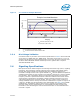
2.7 Clock Specifications
2.7.1 Front Side Bus Clock (BCLK[1:0]) and Processor Clocking
BCLK[1:0] directly controls the FSB interface speed as well as the core frequency of the
processor. As in previous generation processors, the processor’s core frequency is a
multiple of the BCLK[1:0] frequency. The processor bus ratio multiplier will be set at its
default ratio during manufacturing. Refer to Table 14 for the processor supported
ratios.
The processor uses a differential clocking implementation. For more information on the
processor clocking, contact your Intel field representative.
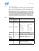
Table 13. GTL+ Bus Voltage Definitions
Symbol Parameter Min Typ Max Units Notes
1
NOTES:
1. Unless otherwise noted, all specifications in this table apply to all processor frequencies.
GTLREF_PU
GTLREF pull up on 975X
and 96x chipset family
boards
124 * 0.99 124 124 * 1.01 Ω
2
2. GTLREF is to be generated from V
TT
by a voltage divider of 1% resistors (one divider for each
GTLEREF land). Refer to the applicable platform design guide for implementation details.
GTLREF_PD
GTLREF pull down on 975X
and 96x chipset family
boards
210 * 0.99 210 210 * 1.01 Ω
2
GTLREF_PU
GTLREF pull up on
Bearlake chipset family
boards
100 * 0.99 100 100 * 1.01 Ω
2
GTLREF_PD
GTLREF pull down resistor
on Bearlake chipset family
boards
200 * 0.99 200 200 * 1.01 Ω
2
R
TT
Termination Resistance 45 50 55 Ω
3
3. R
TT
is the on-die termination resistance measured at V
TT
/3 of the GTL+ output driver.
COMP[3:0] COMP Resistance 49.40 49.90 50.40 Ω
4
4. COMP resistance must be provided on the system board with 1% resistors. See the applicable
platform design guide
for implementation details. COMP[3:0] and COMP8 resistors are to V
SS
.
COMP8 COMP Resistance 24.65 24.90 25.15 Ω
4