
Datasheet


PCI Express* Configuration Registers
496 Intel® Xeon® Processor D-1500 Product Family
Datasheet - Volume 1 of 4: Integrated Platform Controller Hub
March 2015
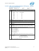
13.1.35 RSTS—Root Status Register (PCI Express*—D28:F0/F1/
F2/F3/F4/F5/F6/F7)
Address Offset: 60h–63h Attribute: R/WC, RO
Default Value: 00000000h Size: 32 bits
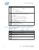
13.1.36 DCAP2—Device Capabilities 2 Register (PCI Express*—
D28:F0/F1/F2/F3/F4/F5/F6/F7)
Address Offset: 64h–67h Attribute: RWO, RO
Default Value: 00080816h Size: 32 bits
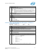
1 System Error on Non-Fatal Error Enable (SNE) — R/W.
0 = An SERR# will not be generated.
1 = An SERR# will be generated, assuming CMD.SEE (D28:F0~F7:04, bit 8) is set, if a non-fatal
error is reported by any of the devices in the hierarchy of this root port, including non-fatal
errors in this root port.
0 System Error on Correctable Error Enable (SCE) — R/W.
0 = An SERR# will not be generated.
1 = An SERR# will be generated, assuming CMD.SEE (D28:F0~F7:04, bit 8) if a correctable error is
reported by any of the devices in the hierarchy of this root port, including correctable errors in
this root port.
Bit Description
Bit Description
31:18 Reserved
17 PME Pending (PP) — RO.
0 = When the original PME is cleared by software, it will be set again, the requestor ID will be
updated, and this bit will be cleared.
1 = Indicates another PME is pending when the PME status bit is set.
16 PME Status (PS) — R/WC.
0 = PME was not asserted.
1 = Indicates that PME was asserted by the requestor ID in RID. Subsequent PMEs are kept pending
until this bit is cleared.
15:0 PME Requestor ID (RID) — RO. Indicates the PCI requestor ID of the last PME requestor. Valid
only when PS is set.
Bit Description
31:12 Reserved
11 LTR Mechanism Supported (LTRMS) — RWO. A value of 1b
indicates support for the optional Latency Tolerance Reporting (LTR) mechanism.
10:5 Reserved
4 Completion Timeout Disable Supported (CTDS) — RO. A value of 1b
indicates support for the Completion Timeout Disable mechanism.
3:0 Completion Timeout Ranges Supported (CTRS) – RO. This field indicates device support for the
optional Completion Timeout programmability mechanism. This mechanism allows system software
to modify the Completion Timeout value.
This field is hardwired to support 10 ms to 250 ms and 250 ms to 4 s.