
Datasheet


xHCI Controller Registers (D20:F0)
Intel® Xeon® Processor D-1500 Product Family 433
Datasheet - Volume 1 of 4: Integrated Platform Controller Hub
March 2015
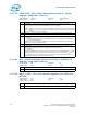
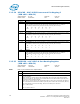
11.2.27 MSI_MCTL— MSI Message Control Register (USB xHCI—
D20:F0)
Address Offset: 82h-83h Attribute: RO, R/W
Default Value: 0086h Size: 16 bits
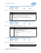
11.2.28 MSI_LMAD—MSI Lower Message Address Register
(USB xHCI—D20:F0)
Address Offset: 84h-87h Attribute: R/W, RO
Default Value: 00000000h Size: 32 bits
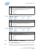
11.2.29 MSI_UMAD—MSI Upper Message Address Register
(USB xHCI—D20:F0)
Address Offset: 88h-8Bh Attribute: R/W
Default Value: 00000000h Size: 32 bits
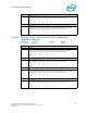
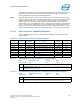
11.2.30 MSI_MD—MSI Message Data Register (USB xHCI—D20:F0)
Address Offset: 8Ch-8Fh Attribute: R/W
Default Value: 00000000h Size: 32 bits
Bit Description
15:8 Reserved.
7 64 Bit Address Capable (C64) — RO. Capable of generating 64-bit messages.
6:4 Multiple Message Enable (MME) — RW. Indicates the number of messages the controller should
assert. This device supports multiple message MSI.
3:1 Multiple Message Capable (MMC) — RO. This field is set by HW to reflect the number of
Interrupters supported. The controller supports up to 8 interrupters.
Encoding for number of Interrupters:
000 1
001 2
010 4
011 8
100 16
101 32
110-111 Reserved
0 MSI Enable (MSIE) — RW. If set to 1, MSI is enabled and the traditional interrupt pins are not used
to generate interrupts.
If cleared to 0, MSI operation is disabled and the traditional interrupt pins are used.
Bit Description
31:2 Lower Message Address — RW. Lower DWord of the system specified message address.
1:0 Reserved.
Bit Description
31:0 Upper Message Address — RW. Upper DWord of the system specified message address.
Bit Description
31:16 Reserved.
15:0 Data — R/W. This 16-bit field is programmed by system software if MSI is enabled. Its content is
driven onto the lower word (PCI AD[15:0]) during the data phase of the MSI memory write
transaction.