
Datasheet


LPC Interface Bridge Registers (D31:F0)
Intel® Xeon® Processor D-1500 Product Family 279
Datasheet - Volume 1 of 4: Integrated Platform Controller Hub
March 2015
73h is used as the data register. Index addresses above 127h are not valid. If the
extended RAM is not needed, it may be disabled.
2. Software must preserve the value of bit 7 at I/O addresses 70h and 74h. When
writing to this address, software must first read the value, and then write the same
value for bit 7 during the sequential address write. Port 70h is not directly readable.
The only way to read this register is through Alt Access mode. Although RTC Index
bits 6:0 are readable from port 74h, bit 7 will always return 0. If the NMI# enable
is not changed during normal operation, software can alternatively read this bit
once and then retain the value for all subsequent writes to port 70h.
7.6.2 Indexed Registers
The RTC contains two sets of indexed registers that are accessed using the two
separate Index and Target registers (70/71h or 72/73h), as shown in Tab l e 7- 7 .
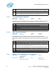
7.6.2.1 RTC_REGA—Register A
RTC Index: 0A Attribute: R/W
Default Value: Undefined Size: 8 bits
Lockable: No Power Well: RTC
This register is used for general configuration of the RTC functions. None of the bits are
affected by RSMRST# or any other Intel® Xeon® Processor D-1500 Product Family
reset signal.
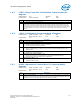
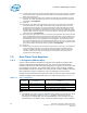
Table 7-7. RTC (Standard) RAM Bank
Index Name
00h Seconds
01h Seconds Alarm
02h Minutes
03h Minutes Alarm
04h Hours
05h Hours Alarm
06h Day of Week
07h Day of Month
08h Month
09h Year
0Ah Register A
0Bh Register B
0Ch Register C
0Dh Register D
0Eh–7Fh 114 Bytes of User RAM
Bit Description
7 Update In Progress (UIP) — R/W. This bit may be monitored as a status flag.
0 = The update cycle will not start for at least 488 µs. The time, calendar, and alarm information in
RAM is always available when the UIP bit is 0.
1 = The update is soon to occur or is in progress.