
Datasheet


LPC Interface Bridge Registers (D31:F0)
256 Intel® Xeon® Processor D-1500 Product Family
Datasheet - Volume 1 of 4: Integrated Platform Controller Hub
March 2015
Note: This register effects the BIOS decode regardless of whether the BIOS is resident on LPC or SPI. The
concept of Feature Space does not apply to SPI-based flash. Intel® Xeon® Processor D-1500 Product
Family simply decodes these ranges as memory accesses when enabled for the SPI flash interface.
7.1.33 BIOS_CNTL—BIOS Control Register (LPC I/F—D31:F0)
Offset Address: DCh Attribute: R/WLO, R/W, RO
Default Value: 20h Size: 8 bits
Lockable: No Power Well: Core
0 BIOS_40_EN — R/W. Enables decoding two 1-M BIOS memory ranges.
0 = Disable.
1 = Enable the following ranges for the BIOS
FF40 0000h–FF4F FFFFh
FF00 0000h–FF0F FFFFh
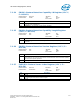
Bit Description
Bit Description
7:6 Reserved
5 SMM BIOS Write Protect Disable (SMM_BWP)— R/WL.
This bit set defines when the BIOS region can be written by the host.
0 = BIOS region SMM protection is disabled. The BIOS Region is writable regardless if processors
are in SMM or not. (Set this field to 0 for legacy behavior).
1 = BIOS region SMM protection is enabled. The BIOS Region is not writable unless all processors
are in SMM and BIOS Write Enable (BIOSWE) is set to ‘1’.
4 Top Swap Status (TSS) — RO. This bit provides a read-only path to view the state of the Top Swap
bit that is at offset 3414h, bit 0.
3:2 SPI Read Configuration (SRC) — R/W. This 2-bit field controls two policies related to BIOS reads
on the SPI interface:
Bit 3 – Prefetch Enable
Bit 2 – Cache Disable
Settings are summarized below:
1 BIOS Lock Enable (BLE) — R/WLO.
0 = Transition of BIOSWE from ‘0’ to ‘1’ will not cause an SMI to be asserted.
1 = Enables setting the BIOSWE bit to cause SMIs and locks SMM_BWP. Once set, this bit can only
be cleared by a PLTRST#.
0 BIOS Write Enable (BIOSWE) — R/W.
0 = Only read cycles result in Firmware Hub or SPI I/F cycles.
1 = Access to the BIOS space is enabled for both read and write cycles. When this bit is written from
a 0 to a 1 and BIOS Lock Enable (BLE) is also set, an SMI# is generated. This ensures that only
SMI code can update BIOS.
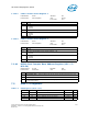
Bits 3:2 Description
00b No prefetching, but caching enabled. 64B demand reads load the read
buffer cache with “valid” data, allowing repeated code fetches to the same line
to complete quickly.
01b No prefetching and no caching. One-to-one correspondence of host BIOS
reads to SPI cycles. This value can be used to invalidate the cache.
10b Prefetching and Caching enabled. This mode is used for long sequences of
short reads to consecutive addresses (that is, shadowing).
11b Reserved. This is an invalid configuration, caching must be enabled when
prefetching is enabled.