
Datasheet


Chipset Configuration Registers
218 Intel® Xeon® Processor D-1500 Product Family
Datasheet - Volume 1 of 4: Integrated Platform Controller Hub
March 2015
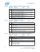
5.1.62 BUC—Backed Up Control Register
Offset Address: 3414h Attribute: R/W
Default Value: 0000000xb Size: 8-bit
All bits in this register are in the RTC well and only cleared by RTCRST#.
2 Reserved Page Route (RPR) — R/W. Determines where to send the reserved page registers.
These addresses are sent to PCI or LPC for the purpose of generating POST codes. The I/O
addresses modified by this field are: 80h, 84h, 85h, 86h, 88h, 8Ch, 8Dh, and 8Eh.
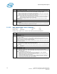
0 = Writes will be forwarded to LPC, shadowed within Intel® Xeon® Processor D-1500 Product
Family, and reads will be returned from the internal shadow
1 = Writes will be forwarded to PCI, shadowed within Intel® Xeon® Processor D-1500 Product
Family, and reads will be returned from the internal shadow.
Note: if some writes are done to LPC/PCI to these I/O ranges, and then this bit is flipped, such
that writes will now go to the other interface, the reads will not return what was last
written. Shadowing is performed on each interface.
The aliases for these registers, at 90h, 94h, 95h, 96h, 98h, 9Ch, 9Dh, and 9Eh, are always
decoded to LPC.
1Reserved
0 BIOS Interface Lock-Down (BILD) — R/WLO.
0 = Disabled.
1 = Prevents BUC.TS (offset 3414, bit 0) and GCS.BBS (offset 3410h, bits 11:10) from being
changed. This bit can only be written from 0 to 1 once.
Bit Description
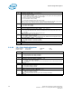
Bit Description
7:6 Reserved
5 LAN Disable — R/W.
0 = LAN is Enabled
1 = LAN is Disabled.
Changing the internal GbE controller from disabled to enabled requires a system reset (write of
0Eh to CF9h (RST_CNT Register)) immediately after clearing the LAN disable bit. A reset is not
required if changing the bit from enabled to disabled.
This bit is locked by the Function Disable SUS Well Lockdown register. Once locked, this bit cannot
be changed by software.
4 Daylight Savings Override (SDO) — R/W.
0 = Daylight Savings is Enabled and configurable by software.
1 = The DSE bit in RTC Register B bit[0] is set to Read-only with a value of 0 to disable daylight
savings.
Note: System BIOS shall configure this bit accordingly during the boot process before RTC time
is initialized.
3:1 Reserved
0 Top Swap (TS) — R/W.
0 = Intel® Xeon® Processor D-1500 Product Family will not allow invert the boot block.
1 = Intel® Xeon® Processor D-1500 Product Family will allow boot block invert, for cycles going
to the BIOS space.
Note: If Top Swap is enabled (TS = 1b):
1. If booting from SPI, then the BIOS boot block size (BOOT_BLOCK_SIZE) soft strap
determines if A16, A17, A18, A19 or A20 should be inverted.
2. If booting from LPC (FWH), then the boot-block size is hard-set to 64 KB and only A16 is
inverted (soft strap is ignored in this case).
3. If Intel® Xeon® Processor D-1500 Product Family is strapped for Top Swap (GPIO55 is low
at rising edge of PCH_PWROK), then this bit cannot be cleared by software. The strap
jumper should be removed and the system rebooted.