
Guide


Mobile Intel Pentium 4 Processor–M and Mobile Intel Celeron Processor FSB Design Guidelines
R
50 Intel
®
852GM Chipset Platform Design Guide
Processor lengths GMCH Lengths
D[62]# AA22 0.268 HD[62]# D16 509
D[63]# AA24 0.394 HD[63]# C18 579
DBI[3]# V21 0.202 DINV[3]# G19 431
4.5.1. Mobile Intel Pentium 4 Processor-M GTLREF Layout and
Routing Recommendations
There are four AGTL+ GTLREF pins on the processor that are used to set the reference voltage level for
the AGTL+ signals (GTLREF). Because all of these pins are connected inside the processor package,
the GTLREF voltage only needs to be supplied to one of the four pins. The other three pins can be left
unconnected.
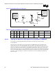
Figure 18. GTLREF Routing
49.9 ohms
1%
1
µ
F
VCC_CPU
pin
Tline
100 ohms
1%
220 pF
L1 = 1.5" max
• The processor must have one dedicated voltage divider.
• Decouple the voltage divider with a 1-µF capacitor.
• Keep the voltage divider within 1.5 inches of the GTLREF pin
• Decouple each pin with a high frequency capacitor (such as a 220 pF 603) as close to the pin as
possible
• Keep signal routing at least 10 mils separated from the GTLREF routes. Use a minimum of a 7-mil
trace for routing.
• Do not allow signal lines to use the GTLREF routing as part of their return path (i.e., do not allow
the GTLREF routing to create splits or discontinuities in the reference planes of the Front Side Bus
signals.)
4.5.2. AGTL+ I/O Buffer Compensation
The Mobile Intel Pentium 4 Processor–M has 2 pins, COMP[1:0], and the Intel 852GM chipset GMCH
has 2 pins, HXRCOMP and HYRCOMP, that require compensation resistors to adjust the AGTL+ I/O
buffer characteristics to specific board and operating environment characteristics. Also, the GMCH
requires two special reference voltage generation circuits to pins HXSWING and HYSWING for the