
Guide


System Memory Design Guidelines (DDR-SDRAM)
R
100 Intel
®
852GM Chipset Platform Design Guide
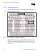
7.3.4.6. DDR Data Routing Example
Figure 49 is an example of a board routing for the Data signal group. The majority of the Data signal
route is on an internal layer, both external layers can be used for parallel termination R-pack placement.
Figure 49. Data Signals Group Routing Example
7.3.5. Control Signals – SCKE[3:0], SCS#[3:0]
The Intel 852GM GMCH chipset control signals, SCKE[3:0] and SCS#[3:0], are clocked into the DDR
SDRAM devices using clock signals SCK/SCK#[5:0]. The GMCH drives the control and clock signals
together, with the clocks crossing in the valid control window. The GMCH provides one chip select
(CS) and one clock enable (CKE) signal per SO-DIMM physical device row. Two chip select and two
clock enable signals will be routed to each SO-DIMM. Refer to Table 38 for the CKE and CS# signal to
SO-DIMM mapping.
Data Signals
From GMCH