
Datasheet


Processor Configuration Registers
200 Datasheet, Volume 2
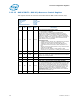
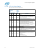
2.12.20 LCTL—Link Control Register
This register allows control of PCI Express link.
B/D/F/Type: 0/0/0/DMIBAR
Address Offset: 88–89h
Reset Value: 0000h
Access: RW, RW-V
Size: 16 bits
BIOS Optimal Default 000h
Bit Attr
Reset
Value
RST/
PWR
Description
15:10 RO 0h Reserved
9RW 0bUncore
Hardware Autonomous Width Disable (HAWD)
When set, this bit disables hardware from changing the Link width
for reasons other than attempting to correct unreliable Link
operation by reducing Link width.
Devices that do not implement the ability autonomously to change
Link width are permitted to hardwire this bit to 0b.
8RO 0h Reserved
7RW 0bUncore
Extended Synch (ES)
0 = Standard Fast Training Sequence (FTS).
1 = Forces the transmission of additional ordered sets when
exiting the L0s state and when in the Recovery state.
This mode provides external devices (such as, logic analyzers)
monitoring the Link time to achieve bit and symbol lock before the
link enters L0 and resumes communication.
This is a test mode only and may cause other undesired side
effects such as buffer overflows or underruns.
6RO 0h Reserved
5RW-V 0bUncore
Retrain Link (RL)
0 = Normal operation.
1 = Full Link retraining is initiated by directing the Physical Layer
TXTSSM from L0, L0s, or L1 states to the Recovery state.
This bit always returns 0 when read. This bit is cleared
automatically (no need to write a 0).
4:2 RO 0h Reserved
1:0 RW 00b Uncore
Active State PM (ASPM):
This field controls the level of active state power management
supported on the given link.
00 = Disabled
01 = L0s Entry Supported
10 = Reserved
11 = L0s and L1 Entry Supported