
Datasheet


Register Description
R
160 Datasheet
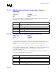
3.11.22 GCCC ⎯ GMCH Clock Control Register
Address Offset: F0–F1h
Default Value: 00 00h
Access: Read/Write
Size: 16 bits
Bit Description
15:10 Reserved
9 Core Display Clock Gate Control (CD-Gate):
0 = Core Display Clock Trunk not Gated, Clock running to the Core.
1 = Core Display Clock Trunk Gated, Clock not running to the Core.
8 Core Render Clock Gate Control (CR-Gate):
0 = Core Render Clock Trunk not Gated, clock running to the core.
1 = Core Render Clock Trunk Gated, clock not running to the core.
7 Reserved
6 Core Display Clock Control (CDCC):
0 = Core Display Clock = Core High Clock (CH).
1 = Core Display Clock = Core Low Clock (CL).
NOTE: This bit can be set to a 1 only when CRCC is set to 01. Setting this to a 1’with
any other combination of CRCC can cause irrecoverable failures.
Gate both core Render and Display Clocks using CR Gate and CD Gate Registers, then
change the value of CDCC Register and update CR Gate and CD Gate to re-enable the
Clocks.
5:4 Core Render Clock Control (CRCC):
00 = Core Render Clock = Core High Clock (CH).
01 = Core Render Clock = Core Low Clock (CL).
10 = Reserved
11 = Reserved
NOTE: CRCC defaults to 00 (CH) and only certain transitions are allowed.
00 Æ 01
01 Æ 00
Gate Core Render Clock using CR Gate Register, then change the value of CRCC
Register and update CR Gate to re-enable the Clock.
3:0 Reserved
§