LXD386 — Evaluation Board for Quad T1/E1 Applications Developer Manual January 2001 As of January 15, 2001, this document replaces the Level One document LXD386 — Evaluation Board for Quad T1/E1 Applications User Guide.
Information in this document is provided in connection with Intel® products. No license, express or implied, by estoppel or otherwise, to any intellectual property rights is granted by this document.
Contents 1.0 General Description .................................................................................................. 5 1.1 2.0 Overview ........................................................................................................................ 7 2.1 2.2 2.3 2.4 3.0 LXD386 Packing List ............................................................................................. 7 Equipment Requirements...........................................................................
5.0 Evaluation Board Schematics............................................................................. 20 Figures 1 2 3 4 5 6 7 8 9 10 11 12 13 14 LXD386 Evaluation Board..................................................................................... 6 Default Switch Settings ...................................................................................... 11 Jumper Block JP5 ...............................................................................................
Evaluation Board for Quad T1/E1 Applications — LXD386 1.0 General Description The LXD386 evaluation board is a versatile tool for engineers designing T1/E1 short haul applications using the LXT386. The evaluation board operates in one of two modes: Software (Host) mode or Hardware mode. In Software mode, the device is controlled with the PC based configuration and monitoring software through an i8051 microcontroller interface.
LXD386 — Evaluation Board for Quad T1/E1 Applications Figure 1.
Evaluation Board for Quad T1/E1 Applications — LXD386 2.0 Caution: Overview CMOS devices are static (ESD) sensitive. Take all industry standard precautions when handling the evaluation board, LXT386 chip, and other sensitive electronic components. Before proceeding with any evaluation board operations, review the specifications for the LXT386 transceiver. 2.1 LXD386 Packing List The evaluation board kit contains the following components: • • • • • • • 2.
LXD386 — Evaluation Board for Quad T1/E1 Applications 2.4 Factory Settings When shipped from the factory, the LXD386 evaluation board’s switches and jumpers are set for software mode and parallel microprocessor interface.
Evaluation Board for Quad T1/E1 Applications — LXD386 3.0 Hardware Mode Set-Up and Operation 3.1 Power Connections The evaluation board has two power planes (VCC and TVCC) each of which is tied to a separate red colored banana jack. 1. Connect the +3.3 VDC power supply to the VCC jack. 2. Connect either a +3.3 VDC or +5.0 VDC power supply to the TVCC jack. 3. Connect the power supply ground lead(s) to the black (GND) banana jack.
LXD386 — Evaluation Board for Quad T1/E1 Applications 3.5 Output Enable Selection The OE switch in switch block S4 controls the operation of the LXT386 output drivers. For normal operation (driver outputs enabled), set the OE switch to the ON position. Setting the OE switch to OFF forces the output drivers to the high impedance state. 3.6 Code Selection In Hardware mode, the MO-INT-CO switch in switch block S4 selects the line encode/decode. To select AMI encode/decode set to the ON position.
Evaluation Board for Quad T1/E1 Applications — LXD386 Figure 2. Default Switch Settings S3 O F F 1 2 3 CLKE OE MO-INT-CO 4 MUX S4 O F F 1 2 3 A0 A1 A2 4 A3 S2 O F F 1 2 3 S1 LOOP2 LOOP3 LOOP4 LOOP5 3 LOOP6 LOOP7 MODE JASEL 7 2 1 NOTE: OFF position = Low = ’0’ 4 5 6 8 9 10 3.9 HIGH LOOP0 LOOP1 4 LOW LEN2 LEN1 LEN0 Line Buildout Selection Switch block S2 is used to select the transmit pulse shaping for T1 mode operation, as well as T1/ E1 mode selection.
LXD386 — Evaluation Board for Quad T1/E1 Applications Figure 3. Jumper Block JP5 3.11 JTAG Boundary Scan Port The eight pin connector JP2 shown in Figure 4 provides access to the IEEE 1149.1 compliant JTAG boundary scan port for board testing purposes. Figure 4. Jumper Block JP2 3.12 Framer/ASIC Connection Ten pin connectors provide access to the digital signals necessary for interfacing with the back-end Framer/Mapper or ASIC.
Evaluation Board for Quad T1/E1 Applications — LXD386 Figure 5. Jumper Block JP 31 3.13 LED Indicators Loss of Signal (LOS) status for each channel is indicated by four LEDs, labeled D3 through D6. If the board is being used in the Software mode, the state of these LEDs will also be displayed on the registers display screen. 3.14 Line Interface Access to the line interface is provided through the green and white banana jacks.
LXD386 — Evaluation Board for Quad T1/E1 Applications 4.0 Software Mode Set-Up and Operation 4.1 i8051 Microcontroller Board An i8051 microcontroller interface board is provided with the evaluation board kit. Connect the i8051 microcontroller board to the evaluation board at the 96 pin header labeled CON1. Connect the microcontroller board to an available serial (COM) port on your PC using the cable provided in the evaluation board kit.
Evaluation Board for Quad T1/E1 Applications — LXD386 4.5 Evaluation Board Software When operating the evaluation board in the software mode, the software provided with the kit will be used to configure the LXT386 and to monitor its operation. This software provides a point-andclick, user friendly interface with on-line help screens. Refer to the data sheet for detailed information about the LXT386 transceiver. 4.
LXD386 — Evaluation Board for Quad T1/E1 Applications Figure 6. Hardware Set-up Screen 4.9 Configuration Screen The configuration screen shown in Figure 7 is the next screen to appear on the monitor. It is the primary control interface with the evaluation board. A graphical representation of each channel is shown in a tabbed display box, along with the control buttons described in the following paragraphs. 4.9.
Evaluation Board for Quad T1/E1 Applications — LXD386 4.9.4 Apply to all Channels Clicking the “Apply to All Channels” control button will configure the other three channels to the settings displayed for the currently selected channel. 4.9.5 Exit The exit control button can be used at any time to close the software. Figure 7.
LXD386 — Evaluation Board for Quad T1/E1 Applications 4.10 Registers Screen 4.10.1 Setting Registers The Registers screen (see in Figure 8) allows direct control of all the LXT386 registers. Each register is labeled by its functional name and hex address. Right click on a register name for on-line help. 4.10.2 Status Indicators Display boxes within the Registers screen show the state settings for individual bit positions of each register.
Evaluation Board for Quad T1/E1 Applications — LXD386 Figure 8.
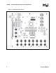
R/W/RD CS OE ALE/SCLK/AS DS/WR/SDI MUX MOT/INTL a32 a31 a30 a29 a28 a27 a26 a25 a24 a23 a22 a21 a20 a19 a18 a17 a16 a15 a14 a13 a12 a11 a10 a9 a8 a7 a6 a5 a4 a3 a2 a1 ALE/SCLK/AS MOT/INTL MUX VCC LOOP1/D1 LOOP3/D3 DLOOP1/D5 DLOOP3/D7 A1 A3 R/W/RD CS OE ALE/SCLK/AS DS/WR/SDI INT ACK/RDY/SDO MUX MOT/INTL 96 Pin DIN Connector Male 32 31 30 29 28 27 26 25 24 23 22 21 20 19 18 17 16 15 14 13 12 11 10 9 8 7 6 5 4 3 2 1 b32 b31 b30 b29 b28 b27 b26 b25 b24 b23 b22 b21 b20 b19 b18 b17 b16 b15 b14 b13 b12 b
TCLK3 TPOS3/TDATA3 TNEG3/UBS3 RCLK3 RPOS3/RDATA3 RNEG3/BPV3 TCLK2 TPOS2/TDATA2 TNEG2/UBS2 RCLK2 RPOS2/RDATA2 RNEG2/BPV2 TCLK1 TPOS1/TDATA1 TNEG1/UBS1 RCLK1 RPOS1/RDATA1 RNEG1/BPV1 TCLK0 TPOS0/TDATA0 TNEG0/UBS0 RCLK0 RPOS0/RDATA0 RNEG0/BPV0 57 56 55 54 53 52 64 63 62 61 60 59 12 13 14 15 16 17 19 20 21 22 23 24 LXT386 TCLK3 TPOS3/TDATA3 TNEG3/UBS3 RCLK3 RPOS3/RDATA3 RNEG3/BPV3 TCLK2 TPOS2/TDATA2 TNEG2/UBS2 RCLK2 RPOS2/RDATA2 RNEG2/BPV2 TCLK1 TPOS1/TDATA1 TNEG1/UBS1 RCLK1 RPOS1/RDATA1 RNEG1/BPV1 T
19 17 15 13 11 9 7 5 3 1 PROTECTED MONITORING ADDRESS SELECT VCC 1 2 3 4 1 2 3 4 1 2 3 4 Hardware mode JA Select 20 18 16 14 12 10 8 6 4 2 LINE BUILDOUTS CS DLOOP3/D7 DLOOP2/D6 DLOOP1/D5 DLOOP0/D4 LOOP3/D3 LOOP2/D2 LOOP1/D1 LOOP0/D0 JP4 HEADER 10X2 SW DIP-4 SW DIP-4 S4 SW DIP-4 S3 S2 8 7 6 5 8 7 6 5 8 7 6 5 CLKE OE MOT/INT/CODEN MUX LEN0 LEN1 LEN2 SWLOOP7 SWLOOP6 SWLOOP5 SWLOOP4 SWLOOP3 SWLOOP2 SWLOOP1 SWLOOP0 MODE R17 4.7k 1 2 3 4 5 6 7 8 9 10 R18 4.7k R19 4.
LOS3 LOS2 LOS1 LOS0 R35 25K R30 25K R29 25K R28 25K VCC VCC VCC + + Developer Manual + + VCC 14 6 14 9 10 11 47uF TANT 7 C29 6 1 2 3 47uF TANT 15 C28 9 10 11 47uF TANT 7 C27 1 2 3 47uF TANT 15 C26 U2A 74LS221 A B CLR REXT/CEXT CEXT U5B 74LS221 A B CLR REXT/CEXT CEXT U5A 74LS221 A B CLR REXT/CEXT CEXT U2B 74LS221 A B CLR REXT/CEXT CEXT Q Q Q Q Q Q Q Q 12 13 12 10 4 5 9 5 13 4 12 2 4 5 1 13 74LS32 U3D 74LS32 U3C 74LS32 U3B 74LS3
RRING1 RTIP1 TTIP2 TRING2 RTIP2 RRING2 TRING3 TTIP3 RRING3 RTIP3 D18 D16 TVCC TVCC R43 D14 D12 R54 1K C34 .22uF 15 Ohms 15 Ohms R39 15 Ohms R41 R53 15 Ohms R50 15 Ohms JP8 11 Ohms R45 11 Ohms R47 560pF C33 5 R52 T2B T2C TG-49-1505-NX 15 14 11 12 13 38 37 36 39 40 28 27 26 29 30 33 32 31 34 35 TG-49-1505-NX T2A TG-49-1505-NX 10 9 6 7 8 4 15 Ohms C37 1 2 3 R51 560pF JP10 JP14 11 Ohms R59 11 Ohms R57 R48 1K TVCC 1K .22uF C35 JP12 .
Developer Manual TCLK3 TPOS3/TDATA3 TNEG3/UBS3 LOS3 TCLK2 TPOS2/TDATA2 TNEG2/UBS2 LOS2 TCLK1 TPOS1/TDATA1 TNEG1/UBS1 LOS1 TCLK0 TPOS0/TDATA0 TNEG0/UBS0 LOS0 R70 100k 100k 100k 100k R69 R67 100k 100k R66 R64 100k 100k R63 R61 R60 100k R71 100k R68 100k R65 100k R62 2 4 6 8 10 2 4 6 8 10 2 4 6 8 10 2 4 6 8 10 HEADER 5X2 1 3 5 7 9 JP18 HEADER 5X2 1 3 5 7 9 JP17 HEADER 5X2 1 3 5 7 9 JP16 HEADER 5X2 1 3 5 7 9 JP15 CHANNEL 3 RCLK3 RPOS3/RDATA3 RNEG3/BPV3 CHANNEL 2 RC