LXD381 — Evaluation Board for Octal E1 Applications Developer Manual January 2001 As of January 15, 2001, this document replaces the Level One document LXD381 — Evaluation Board for Octal E1 Applications User Guide.
Information in this document is provided in connection with Intel® products. No license, express or implied, by estoppel or otherwise, to any intellectual property rights is granted by this document.
Contents 1.0 General Description .................................................................................................. 5 1.1 2.0 Evaluation Board Set-Up ......................................................................................... 7 2.1 2.2 2.3 2.4 2.5 2.6 2.7 2.8 2.9 2.10 2.11 3.0 Features ................................................................................................................ 5 LXD381 Packing List .......................................................
Evaluation Board for Octal E1 Applications — LXD381 1.0 General Description The LXD381 evaluation board is a versatile tool for engineers designing E1 short haul applications using the LXT381. The evaluation board operates in Hardware mode only. All device and channel controls are set using jumper blocks and DIP switches. The board provides banana jacks for both power and line interface connections. Connectors are provided for each framer or back-end ASIC interface.
LXD381 — Evaluation Board for Octal E1 Applications Figure 1.
Evaluation Board for Octal E1 Applications — LXD381 2.0 Caution: Evaluation Board Set-Up CMOS devices are static (ESD) sensitive. Take all industry standard precautions when handling the evaluation board, the LXT381 chip and other sensitive electronic components. Before proceeding with any evaluation board operations, review the specifications for the LXT381 transceiver. 2.1 LXD381 Packing List The evaluation board kit contains the following components: • LXD381 board with LXT381 device installed.
LXD381 — Evaluation Board for Octal E1 Applications 2.5 Receive Polarity Selection The polarity of RPOS/RNEG is determined by the CLKE switch in switch block S2. When the CLKE switch is OFF, RPOS/RNEG are active Low. When set to the ON position, RPOS/RNEG are active High. Note that the CLKE switch controls the LXT381’s RPOL pin. 2.6 Output Enable Selection The OE switch in switch block S3 controls the operation of the LXT381 output drivers.
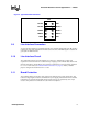
Evaluation Board for Octal E1 Applications — LXD381 Figure 3. Typical Back-End Connector JP1 2.9 TCLK 0 1 2 GND TCLK 0 3 4 RCLK 0 TPOS 0 5 6 RPOS 0 TNEG 0 7 8 RNEG 0 LOS 0 9 10 GND Line Interface Connection Access to the line interface is provided through the green and white banana jacks. The TIP signal is routed to the white jacks for both transmit and receive directions. The RING signal is routed to the green jacks for both directions. 2.
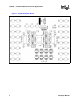
BANANA JACK 3.3 VOLTS GROUND BANANA JACK TVCC R.NETWORK 4.7K CM1 R8 R7 R6 R5 CM2 R4 R3 R2 R1 RN1 10 9 8 7 6 5 4 3 2 1 + - + RED BN3 BLACK RED BN2 BN1 1 1 1 C8 .01uf C6 .01uf 68 uF VCC TVCC C7 C5 68 uF RN1_4 RN1_3 RN1_2 RN1_1 RN1_9 RN1_8 RN1_7 RN1_6 10 9 8 7 6 5 4 3 2 1 TVS 3.3V D2 TVS 5V D1 R.NETWORK 4.7K CM1 R8 R7 R6 R5 CM2 R4 R3 R2 R1 RN2 1 2 3 4 8 7 6 5 VCC RN2_2 RN2_1 SW DIP-4 S2 CLKE OE RN2_8 RN2_9 10 18 4.
Developer Manual R.NETWORK 100K CM1 R8 R7 R6 R5 CM2 R4 R3 R2 R1 RN5 R.NETWORK 100K CM1 R8 R7 R6 R5 CM2 R4 R3 R2 R1 RN4 R.
TRING1 TTIP1 RRING1 RTIP1 TRING0 TTIP0 RRING0 TVCC TVCC TVCC D18 D15 TVCC D13 D10 D6 D4 R13 JP20 R25 R23 11 11 1K R21 1K R17 11 JP18 0.22uF C26 JP14 D17 D8 R11 1K R9 11 JP12 0.
TRING5 TTIP5 RRING5 RTIP5 TRING4 TTIP4 RRING4 TVCC TVCC D34 D31 TVCC D29 D25 D21 TVCC D19 R34 JP32 R49 D33 R47 11 11 1K R45 1K R41 11 JP30 0.22uF C38 JP25 R36 D23 1K R32 1K 11 JP23 0.