Intel® Edison Kit for Arduino* Hardware Guide December 2014 Revision 004 Document Number: 331191-004
Notice: This document contains information on products in the design phase of development. The information here is subject to change without notice. Do not finalize a design with this information. INFORMATION IN THIS DOCUMENT IS PROVIDED IN CONNECTION WITH INTEL PRODUCTS. NO LICENSE, EXPRESS OR IMPLIED, BY ESTOPPEL OR OTHERWISE, TO ANY INTELLECTUAL PROPERTY RIGHTS IS GRANTED BY THIS DOCUMENT.
Contents 1 2 3 4 5 6 7 8 9 10 11 Introduction ....................................................................................................................................................................... 6 1.1 Software requirements ............................................................................................................................................................... 6 1.2 Terminology .......................................................................................
Figures Figure 1 Figure 2 Figure 3 Figure 4 Figure 5 Figure 6 Figure 7 Figure 8 Figure 9 Arduino* Uno* pinout ............................................................................................................................................................. 7 Intel® Edison kit for Arduino* block diagram ............................................................................................................ 13 Intel® Edison kit for Arduino* PWM swizzler ........................................
Revision History Revision Description Date ww32 Initial release August 4, 2014 ww34 Minor edits. August 20, 2014 ww36 Removed a column from Table 2. September 5, 2014 001 First public release. September 9, 2014 002 Minor corrections. September 15, 2014 003 Added product overview chapter and shield pin configuration chapter. September 18, 2014 Updated sections on software recovery mode, pin function mux controls, and LEDs.
Shield pin configuration 1 Introduction This document describes the hardware interface of the Intel® Edison kit for Arduino*. The kit contains external input/output pin connections which may be configured to be used in a variety of interfacing modes, such as GPIO, PWM, SPI, I2C, ADC, for compatibility with Arduino* Uno* shield hardware.
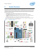
Shield pin configuration 2 Product Overview The 20 Arduino*-compatible shield I/O pins on the Intel® Edison kit for Arduino* are numbered IO0-IO19 (Figure 1). All pins support basic GPIO functionality. Some of the pins also support PWM, ADC, SPI or I2C functions. Selection of different pin functions on the Intel® Edison kit for Arduino* is achieved through use of SoC pin control interfaces and GPIO output signals dedicated for multiplexing control.
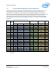
Shield pin configuration 2.1 Shield pin GPIO mapping Table 2 describes the mapping of GPIO and PWM pin numbers (in Linux) to shield I/O pins. The following details are included: • Shield pin. Digital I/O pin number as per Arduino* Uno* pin numbering scheme. • GPIO (Linux). The pin number assigned under Linux. • Muxed functions. Other signals available on this shield pin, as they appear on the schematic.
Shield pin configuration 2.2 Pin function multiplexing control (summary) All GPIO pins on the Arduino* header require some internal GPIOs to be set up before the pin is usable. This is usually as simple as setting an output enable, pullup enable, and mode. However, some pins have extra functionality such as SPI, PWM, or I2C, so these pins need extra multiplexing (muxing) in order to be usable.
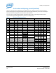
Shield pin configuration 2.3 Pin function multiplexing control (detailed) Table 4 lists the GPIO outputs dedicated to pin multiplexing control. Different functions may be selected for specific shield I/O pins by setting these GPIO outputs to 0/1 (low/high). Additionally, some of the SoC GPIO pins also feature internal mux options. These are listed as “SoC Pin Modes”.
Shield pin configuration 2.4 GPIO interrupt support All GPIO inputs on the Intel® Edison platform are interrupt-capable, and all interrupt types are supported on all inputs. Table 5 lists the specific edge- and level-triggered interrupt types that are supported on each pin. Table 5 Shield pin 1.
Shield pin configuration 2.6 Pin direction and pullup control For most shield pins on the Intel® Edison kit for Arduino*, there is a buffer/level-shifter which needs to be configured for input or output direction, and an external 47 kohm pullup/pulldown resistor, which may be optionally enabled. Both are driven by dedicated GPIO outputs, listed in Table 7. When configuring a shield pin as an output, we advise configuring the buffer for output before setting the SoC GPIO pin direction to output.
Shield pin configuration 3 High-Level Functional Description The Intel® Edison kit for Arduino*expansion board is designed to be hardware and software pin-compatible with Arduino shields designed for the Uno R3. Digital pins 0 to 13 (and the adjacent AREF and GND pins), analog inputs 0 to 5, the power header, ICSP header, and the UART port pins (0 and 1) are all in the same locations as on the Arduino Uno R3. This is also known as the Arduino 1.0 pinout.
Shield pin configuration 3.1 Intel® Edison kit for Arduino* header signal list The Intel® Edison kit for Arduino* digital signals can be configured as input or output. When programmed as an input, a GPIO can serve as an interrupt. The Intel® Edison kit for Arduino* 1.8 V I/O are translated to 3.3 or 5 V using SN74LVC1T45 dual supply bus transceivers with 3 state outputs. Both outputs go tristate if either supply rail is at ground. The port direction is referenced to VCCA.
Shield pin configuration 3.2 Intel® Edison kit for Arduino* PWM swizzler There are four available GPIO that can be configured as PWM outputs. The PWM features are: • The PWM Output Frequency and Duty Cycle can be estimated by the equations: • Target frequency ~= 19.2 MHz * Base_unit value / 256 • Target PWM Duty Cycle ~= PWM_on_time_divisor / 256 The four PWM sources are wired to a PWM “swizzler”.
Shield pin configuration Figure 4 PWM swizzler on the Intel® Edison kit for Arduino* 3.3 Intel® Edison kit for Arduino* analog inputs The analog inputs are fed to an ADS7951 A/D converter. This device has the following features: • 20 MHz clock rate • 12-bit A/D conversion • 1 MHz sample rate • 70 dB signal to noise ratio • 0 to 2.5 V or 0 to 5 V input range (select either AREF or IOREF via jumper J8 onboard) The analog inputs are multiplexed with digital I/O using SN74LVC2G53 analog switches.
Shield pin configuration 3.6 Intel® Edison kit for Arduino* power supply The Intel® Edison compute module is a low power device. In general it will not draw more than 200 mA (approximately 430 mA (final value TBD) when transmitting over Wi-Fi) from the main power source. Therefore, the Intel® Edison kit for Arduino* may run on USB power (when configured as a device), or off an external power adapter from 7 to 15 V. Power from the external power adapter goes to a DC-DC converter and down converted to 5 V.
Shield pin configuration 4 Powering the Intel® Edison kit for Arduino* You can power the Intel® Edison kit for Arduino* using any of the following: • an external power supply on J1; • DCIN via shield header pin VIN; • a USB cable via micro USB connector J16; or • a lithium-ion battery connected to J2. When power is applied to J1 or VIN, the external power must be in the range of 7 to 17 V. The power is converted to 5 V via a switching power supply, which powers the rest of the system.
Shield pin configuration Some considerations of the power distribution in the Intel® Edison kit for Arduino*: • There is a diode ORing of the 5 V DC/DC and the VBUS input. In the case of powering the Intel® Edison kit for Arduino* from VBUS, the shield voltage may be as low as 4.4 V (4.75 V VBUS min – 0.3 V diode drop). In the case of external power adapter, voltage to the shield will be 5 V ±2%. • Using the Intel® Edison compute module as a USB HOST requires use of an external adapter.
Shield pin configuration 5 Batteries The rechargers chosen on the Intel® Edison kit for Arduino* and the Intel® Edison Breakout Board were designed for lithium-ion or lithium-polymer batteries. Follow the manufacturer’s guidelines when charging batteries. Generally, charging current should not exceed 50 to 70% of the rated capacity. For example, a 200 mAH battery should be charged with 70% • 200 mA = (140 mA).
Shield pin configuration 6 Layout 6.1 Antenna keepout The area under and around the antenna should be kept free of all components, routes, and ground plane. The Intel® Edison compute module DXF in white with antenna keepout shown in the Arduino* trace layers. See Figure 7. Figure 7 Area around antenna 6.2 Layout SD card, I2S, SPI, I2C Table 10 Layout SD card Signal parameter Metric (mm) Standard (mils) Total length L1 0.254 to 101.
Shield pin configuration 6.3 LEDs The Intel® Edison kit for Arduino has three LEDs. (See Figure 5 for locations.) • DS1 is the reset LED. It will turn on when the Intel® Edison processor is running. When the processor is in reset and asserting RESET_OUT# low, it will turn off. • DS2 is the standard LED on the Arduino* board. It runs using the ‘blink’ code or whenever Digital I/O 13 is asserted High. It can be used as an indicator under direct control. • DS3 is the battery charging LED.
Shield pin configuration 7 Handling When assembling an Intel® Edison compute module to an Arduino* board, handle the Intel® Edison compute module by the PCB edges. Avoid holding or exerting pressure to the shields. To mate the Intel® Edison compute module to the Arduino* board, apply pressure directly above the connector and to the left corner, as shown in Figure 8.
Shield pin configuration 8 Debug UART and Low-Power Sleep Mode When the Intel® Edison compute module goes into low-power sleep, the UART internal FIFO and interface is powered down. Therefore, a two-wire UART (Rx/Tx) will lose the first received character whenever the Intel® Edison compute module is in low-power sleep mode. In order to avoid this condition, when sleep mode is enabled, a fourwire UART (Rx, Tx, CTS, and RTS) is required.
Shield pin configuration 9 Buttons This section explains the software functionality of the Intel® Edison kit for Arduino* buttons. The Intel® Edison kit for Arduino* has the following buttons: • System reset. Pressing the system reset button (SW1UI5) will reset the Intel® Edison compute module, and reset the I/O expanders, setting all the shield pins to high impedance state with no pullups. • Shield reset.
Shield pin configuration 10 Digikey sources Figure 9 shows some third-party accessories you can use. Figure 9 Digikey sources Mating connector 2.0 mm DF40C(2.0)-70DS-0.4V(51) - H11908CT-ND Cut tape DF40C(2.0)-70DS-0.
Shield pin configuration 11 Shield pin configuration This chapter will help you configure the Arduino* shield pins. To configure the Arduino* shield pins, do the following: 1. Identify the Arduino* shield pin number of the pin you want to use, in the range IO0-IO19. 2. Identify the functions available for the given pin, and select the function you want to use. Typical functions are GPIO, PWM, UART, I2C, SPI, ADC. Only some functions are available on each pin. 3.
Shield pin configuration 11.2 Configure IO11 as a GPIO input, with pullup resistor disabled To configure IO11 as a GPIO input, with pullup resistor disabled, do the following: 1. Refer to Table 2 for the GPIO number. According to Table 2, the GPIO number for IO11 is 43. 2. According to Table 4, GPIO 262 must be set to 1 to select GPIO/SPI, GPIO 241 must be set to 0 to select GPIO, and GPIO 43 pin-mux must be set to ‘mode0’ to select GPIO. 3.
Shield pin configuration 11.4 Configure IO6 as a PWM output To configure IO6 as a PWM output, do the following: 1. Refer to Table 2 for the GPIO number. According to Table 2, the GPIO number for IO6 is 182. 2. According to Table 4, GPIO 182 pin-mux must be set to ‘mode1’ to select PWM. 3. According to Table 7, GPIO 254 must be set to 1 to enable the output direction for IO6. 4. According to Table 7, GPIO 222 must be set as a high-impedance input to disable the pullup resistor for IO6. 5.
Shield pin configuration Configure IO18/IO19 for I2C connectivity 11.6 To configure IO18 and IO19 for I2C connectivity, do the following: 1. Refer to Table 2 for the GPIO numbers. According to Table 2, the GPIO numbers for IO18 and IO19 are 28 and 27, respectively. 2. According to Table 4, GPIO 204 must be set to 1 to select GPIO/I2C, and GPIO 28 pin-mux must be set to ‘mode1’ to select I2C for IO18. 3.
Shield pin configuration 11.7 Configure IO10 through IO13 for SPI connectivity To configure IO10 through IO13 for SPI connectivity, do the following: 1. Refer to Table 2 for the GPIO numbers. According to Table 2, the GPIO numbers for IO10 through IO13 are 111, 115, 114, and 109, respectively. 2. According to Table 4, GPIO 263 must be set to 1 to select GPIO/SPI, GPIO 240 must be set to 1 to select SPI, and GPIO 111 pin-mux must be set to ‘mode1’ to select SPI for IO10. 3.
Shield pin configuration # # # # # # # echo echo echo echo echo echo echo in > /sys/class/gpio/gpio228/direction in > /sys/class/gpio/gpio229/direction mode1 > /sys/kernel/debug/gpio_debug/gpio111/current_pinmux mode1 > /sys/kernel/debug/gpio_debug/gpio115/current_pinmux mode1 > /sys/kernel/debug/gpio_debug/gpio114/current_pinmux mode1 > /sys/kernel/debug/gpio_debug/gpio109/current_pinmux low > /sys/class/gpio/gpio214/direction You should be able to use IO10 through IO13 for SPI connectivity.