
Computer Hardware User Manual

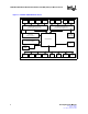
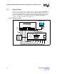
Table Of Contents
- 1.0 General Description
- 2.0 Introduction
- 3.0 Quick-Start Checklist
- 4.0 Optional Configurations
- 5.0 LEDs
- 6.0 Board Schematics
- Figure 4. LXD9785 PQFP MII Demo Board Power (Fiber Board Revision A2)
- Figure 5. Control
- Figure 6. MII Ports 0 and 1
- Figure 7. MII Ports 2 and 3
- Figure 8. MII Ports 4 and 5
- Figure 9. MII Ports 6 and 7
- Figure 10. Fiber Ports 0 and 1
- Figure 11. Fiber Ports 2 and 3
- Figure 12. Fiber Ports 4 and 5
- Figure 13. Fiber Ports 6 and 7
- Figure 14. Caps
- Figure 15. SS-SMII to MII ALTERA
- Figure 16. Clock Distribution
- Figure 17. Inter-Frame Status LEDs
- Figure 18. Logic Analyzer
- Figure 19. MDIO0 and MDC0 Fix
- Figure 20. MDIO1 and MDC1 Fix
- 7.0 Bill of Materials
LXD9785 PQFP Demo Board with FPGA for SS-SMII (Fiber)-to-MII Conversion
8 Development Kit Manual
Document #: 249323
Revision #: 003
Rev. Date: January 24, 2002
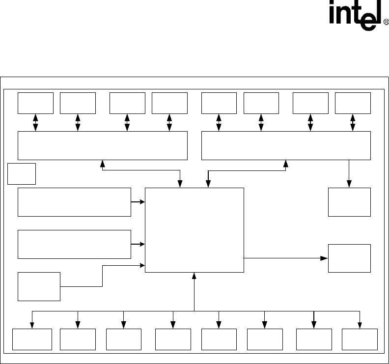
Figure 1. LXD9785 PQFP MII Demo Board
LXT9785/9785E
Port 0 MII
Header
Port 1 MII
Header
Port 2 MII
Header
Port 3 MII
Header
Port 4 MII
Header
Port 5 MII
Header
Port 6 MII
Header
Port 7 MII
Header
Config Logic
Switches & Jumpers
Inter Frame
Status LEDs
FPGA
SS-SMII to MII Converter and
Inter Frame Status Output Connector
FPGA
SS-SMII to MII Converter and
Inter Frame Status Output Connector
REFCLK Clocks
and Clock Distribution
+2.5V &
+3.3V Power
Supply
Direct Drive
LEDs
RJ-11
Port 7 Fiber
Header
Port 6 Fiber
Header
Port 5 Fiber
Header
Port 4 Fiber
Header
Port 3 Fiber
Header
Port 2 Fiber
Header
Port 1 Fiber
Header
Port 0 Fiber
Header