
Computer Hardware User Manual
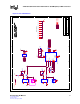
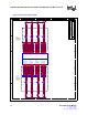
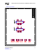
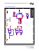
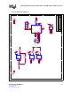
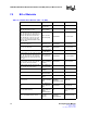
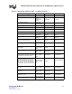
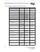

Table Of Contents
- 1.0 General Description
- 2.0 Introduction
- 3.0 Quick-Start Checklist
- 4.0 Optional Configurations
- 5.0 LEDs
- 6.0 Board Schematics
- Figure 4. LXD9785 PQFP MII Demo Board Power (Fiber Board Revision A2)
- Figure 5. Control
- Figure 6. MII Ports 0 and 1
- Figure 7. MII Ports 2 and 3
- Figure 8. MII Ports 4 and 5
- Figure 9. MII Ports 6 and 7
- Figure 10. Fiber Ports 0 and 1
- Figure 11. Fiber Ports 2 and 3
- Figure 12. Fiber Ports 4 and 5
- Figure 13. Fiber Ports 6 and 7
- Figure 14. Caps
- Figure 15. SS-SMII to MII ALTERA
- Figure 16. Clock Distribution
- Figure 17. Inter-Frame Status LEDs
- Figure 18. Logic Analyzer
- Figure 19. MDIO0 and MDC0 Fix
- Figure 20. MDIO1 and MDC1 Fix
- 7.0 Bill of Materials
LXD9785 PQFP Demo Board with FPGA for SS-SMII (Fiber)-to-MII Conversion
Development Kit Manual 39
Document #: 249323
Revision #: 003
Rev. Date: January 24, 2002
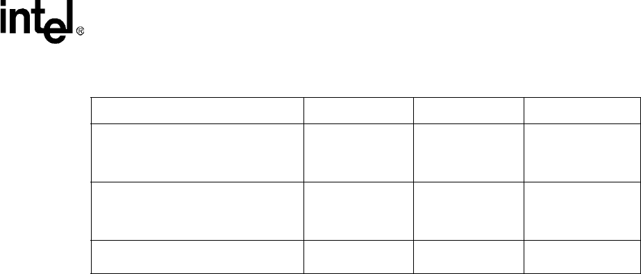
(DO NOT INSTALL U34, 35, 37, 40, 41,
43)
IC LOGIC
NC7SZ125
SINGLE TRISTATE
BUFFER SOT23
FAIRCHILD
SEMICONDUCTOR
NC7SZ125M5
U46 (DO NOT INSTALL U36, 42)
IC FPGA 7032A
3.3V
PROGRAMMABLE
PLD 44 PIN TQFP
ALTERA EPM7032AETC44-4
Y1, 2 (DO NOT INSTALL)
OSC 125.000MHZ
25PPM 3.3V
SARONIX SCS-LO-1067
Table 10. LXD9785 Bill of Materials (Fiber - SS-SMII) (Continued)
Reference Designator Description Manufacturer Part Number