
Computer Hardware User Manual
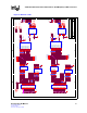
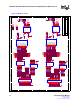
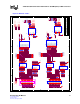
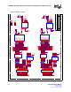
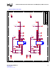
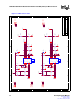
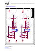
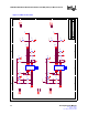
Table Of Contents
- 1.0 General Description
- 2.0 Introduction
- 3.0 Quick-Start Checklist
- 4.0 Optional Configurations
- 5.0 LEDs
- 6.0 Board Schematics
- Figure 4. LXD9785 PQFP MII Demo Board Power (Fiber Board Revision A2)
- Figure 5. Control
- Figure 6. MII Ports 0 and 1
- Figure 7. MII Ports 2 and 3
- Figure 8. MII Ports 4 and 5
- Figure 9. MII Ports 6 and 7
- Figure 10. Fiber Ports 0 and 1
- Figure 11. Fiber Ports 2 and 3
- Figure 12. Fiber Ports 4 and 5
- Figure 13. Fiber Ports 6 and 7
- Figure 14. Caps
- Figure 15. SS-SMII to MII ALTERA
- Figure 16. Clock Distribution
- Figure 17. Inter-Frame Status LEDs
- Figure 18. Logic Analyzer
- Figure 19. MDIO0 and MDC0 Fix
- Figure 20. MDIO1 and MDC1 Fix
- 7.0 Bill of Materials
LXD9785 PQFP Demo Board with FPGA for SS-SMII (Fiber)-to-MII Conversion
26 Development Kit Manual
Document #: 249323
Revision #: 003
Rev. Date: January 24, 2002
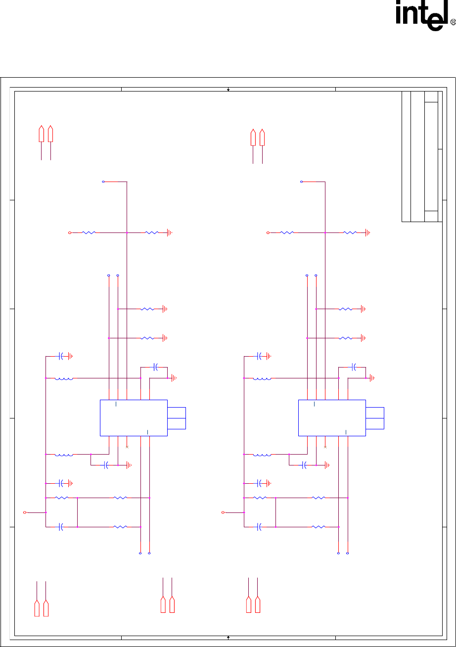
Figure 11. Fiber Ports 2 and 3
A
A
B
B
C
C
D
D
E
E
4 4
3 3
2 2
1 1
FIBER PORTS 2&3 A2
LXD9785 SS/SMII MII FX DV BOARD
B
918Wednesday, February 21, 2001
Title
Size Document Number Rev
Date: Sheet
of
TPFOP2
TPFON2
TPFON3
TPFOP3
TPFIP2
TPFIN2
TPFIP3
TPFIN3
TPFOP2
TPFON2
TPFIN2
TPFIP2
TPFIP3
TPFIN3
TPFON3
SD2
SD3
SD2
SD3
TPFOP3
TPFON2
TPFOP2
TPFOP3
TPFON3
TPFIN2 5
TPFIP2 5
TPFIN3 5
TPFIP3 5
SD3
SD2
GND
GNDGND
GND
GND GND
GND
GND
GND
GND
GND
GND
GND
GND
VCC_FX
VCC_FX
VCC_FX
VCC_FX
+
C298
0.1uF
TP202
1
R674
130
L7
1uH
TP203
1
R675
130
+
C297
0.1uF
TP201
1
L5
1uH
L8
1uH
TP200
1
+
C292
0.1uF
R681
50 1%
TP206
1
+
C291
0.1uF
R682
50 1%
TP207
1
R673
50 1%
+
C295
0.1uF
TP204
1
R672
50 1%
R684
130
TP205
1
+
C288
10uF
+
C289
0.1uF
R676
82
FIBER PORT
F3
HFBR_5903
6
7
8
9
10
5
4
3
2
1
TX Vcc
TX Gnd
N/C
TD
TD
RD
RD
SD
RX Vcc
RX Gnd
R685
82
FIBER PORT
F4
HFBR_5903
6
7
8
9
10
5
4
3
2
1
TX Vcc
TX Gnd
N/C
TD
TD
RD
RD
SD
RX Vcc
RX Gnd
R678
130
R683
130
TP186
1
+
C293
0.1uF
TP187
1
L6
1uH
R669
130
+
C299
0.1uF
R668
27
+
C294
10uF
R677
27