
Computer Hardware User Manual
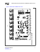
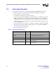
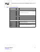
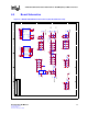
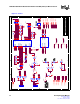
Table Of Contents
- 1.0 General Description
- 2.0 Introduction
- 3.0 Quick-Start Checklist
- 4.0 Optional Configurations
- 5.0 LEDs
- 6.0 Board Schematics
- Figure 4. LXD9785 PQFP MII Demo Board Power (Fiber Board Revision A2)
- Figure 5. Control
- Figure 6. MII Ports 0 and 1
- Figure 7. MII Ports 2 and 3
- Figure 8. MII Ports 4 and 5
- Figure 9. MII Ports 6 and 7
- Figure 10. Fiber Ports 0 and 1
- Figure 11. Fiber Ports 2 and 3
- Figure 12. Fiber Ports 4 and 5
- Figure 13. Fiber Ports 6 and 7
- Figure 14. Caps
- Figure 15. SS-SMII to MII ALTERA
- Figure 16. Clock Distribution
- Figure 17. Inter-Frame Status LEDs
- Figure 18. Logic Analyzer
- Figure 19. MDIO0 and MDC0 Fix
- Figure 20. MDIO1 and MDC1 Fix
- 7.0 Bill of Materials
LXD9785 PQFP Demo Board with FPGA for SS-SMII (Fiber)-to-MII Conversion
Development Kit Manual 13
Document #: 249323
Revision #: 003
Rev. Date: January 24, 2002
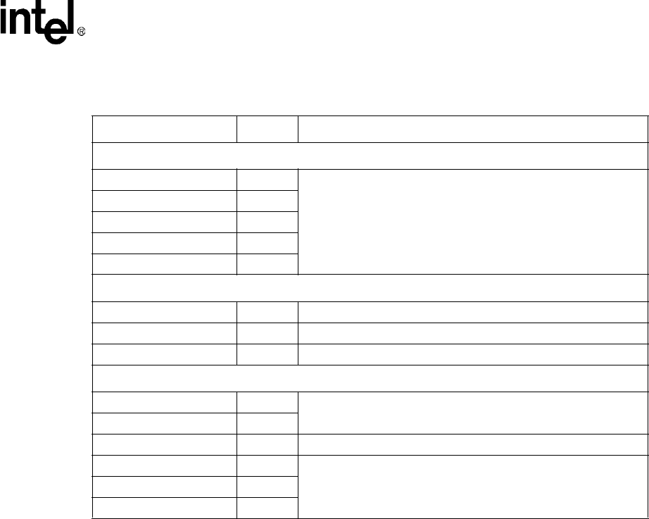
Table 2. Quick-Start Switch Settings
Switch / Label Setting Configuration
Switch S1
S1-1 / ADD_0 0
Sets PHY MDIO base address to 00000.
S1-2 / ADD_1 0
S1-3 / ADD_2 0
S1-4 / ADD_3 0
S1-5 / ADD_4 0
Switch S5
S5-1 / PAUSE 0 Disables Pause function.
S5-2 / PWRDWN 0 Disables Power-Down function.
S5-3 / MDDIS 0 Enables MDIO channel.
Switch S8
S8-1 / ModeSel 0 0
Switch settings for SS-SMII mode.
S8-2 / ModeSel 1 1
S8-3 /Section 0 Enables Section mode: 1x8 or 2x4.
S8-4 / CFG_3 1
Sets port configuration to 100 Mbps and Full-Duplex.S8-5 / CFG_2 1
S8-6 / CFG_1 0