
Computer Hardware User Manual

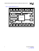
Table Of Contents
- 1.0 General Description
- 2.0 Introduction
- 3.0 Quick-Start Checklist
- 4.0 Optional Configurations
- 5.0 LEDs
- 6.0 Board Schematics
- Figure 4. LXD9785 PQFP MII Demo Board Power (Fiber Board Revision A2)
- Figure 5. Control
- Figure 6. MII Ports 0 and 1
- Figure 7. MII Ports 2 and 3
- Figure 8. MII Ports 4 and 5
- Figure 9. MII Ports 6 and 7
- Figure 10. Fiber Ports 0 and 1
- Figure 11. Fiber Ports 2 and 3
- Figure 12. Fiber Ports 4 and 5
- Figure 13. Fiber Ports 6 and 7
- Figure 14. Caps
- Figure 15. SS-SMII to MII ALTERA
- Figure 16. Clock Distribution
- Figure 17. Inter-Frame Status LEDs
- Figure 18. Logic Analyzer
- Figure 19. MDIO0 and MDC0 Fix
- Figure 20. MDIO1 and MDC1 Fix
- 7.0 Bill of Materials
LXD9785 PQFP Demo Board with FPGA for SS-SMII (Fiber)-to-MII Conversion
10 Development Kit Manual
Document #: 249323
Revision #: 003
Rev. Date: January 24, 2002
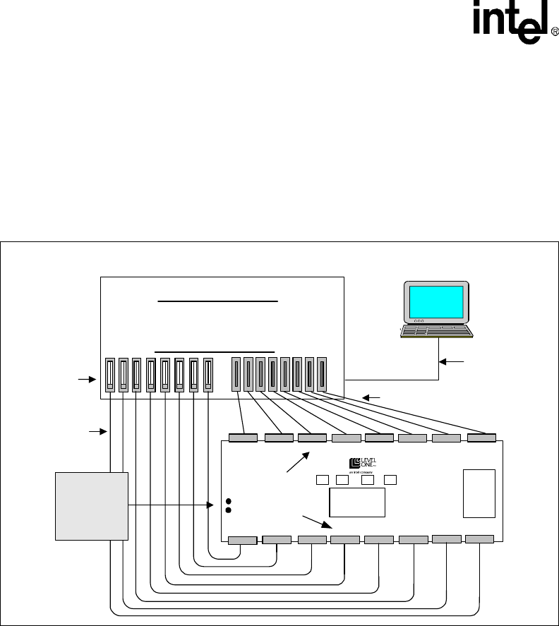
2.4 Typical Setup
Figure 2 shows a typical test setup for standard operation of the LXD9785/9785E PQFP MII Demo
Board. The Demo Board plugs into a SmartBits Advanced Multi-port Performance Test Box via
eight standard 40-pin MII cables (not included on the board). Eight external NIC cards directly
connect to the SmartBits test box and plug into the Demo Board through fiber-module connectors.
Each port’s operation speed is set globally via hardware or individually via the MDIO for
evaluation of 100 Mbps capabilities using all eight ports.
Figure 2. Typical Test Setup
Fiber
SmartBits
Advanced Multi-port
Performance
Tester
Demo Board
MII Cable
External
NIC
Cards
RS-232
LXT9785
/9785E
+2.5V/
+3.3V DC
Power
Supply
Computer Setup
LEDs
MII
Connectors
Smart
Windows
Fiber-Module
Connectors