
Technical Product Specification


Technical Reference
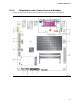
43
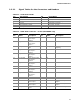
2.2.2.1 Signal Tables for the Connectors and Headers
Table 11. Serial Port Header
Pin
Signal Name
Pin
Signal Name
1 DCD (Data Carrier Detect) 2 RXD# (Receive Data)
3 TXD# (Transmit Data) 4 DTR (Data Terminal Ready)
5 Ground 6 DSR (Data Set Ready)
7 RTS (Request To Send) 8 CTS (Clear To Send)
9 RI (Ring Indicator) 10 Key (no pin)
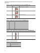
Table 12. LVDS Data Connector - 30-Pin (D525MWV only)
Pin
Signal
Name
Description
Pin
Signal
Name
Description
1 LA_CLKN LVDS Channel A diff
clock output -
negative
2 NC
3 LA_CLKP LVDS Channel A diff
clock output -
positive
4 NC
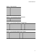
5 EDID_3.3V Power for EDID
ROM
6 EDID_GND Ground for EDID
signaling
7 LA_DATAN0 LVDS Channel A diff
data output –
negative
8 NC
9 LA_DATAP0 LVDS Channel A diff
data output –
positive
10 NC
11 LA_DATAN1 LVDS Channel A diff
data output –
negative
12 NC
13 LA_DATAP1 LVDS Channel A diff
data output –
positive
14 NC
15
GND
Ground
16
GND
Ground
17 LA_DATAN2 LVDS Channel A diff
data output –
negative
18 NC
19 LA_DATAP2 LVDS Channel A diff
data output –
positive
20 NC
21
GND
Ground
22
GND
Ground
23
GND
Ground
24
GND
Ground
25 3.3 V/5 V/12 V Selectable LCD
power output
26 3.3 V/5 V/12 V Selectable LCD power
output
27 3.3 V/5 V/12 V Selectable LCD
power output
28 3.3 V/5 V/12 V Selectable LCD power
output
29 EDID_CLK EDID/DDC clock
signal
30 EDID_DATA EDID/DDC data signal