Intel® LXD972M Transceiver Demo Board (Board Rev A1) Preliminary User’s Guide October 2004 Document Number: 303125 Revision Number: 002 Revision Date: October 22, 2004
INFORMATION IN THIS DOCUMENT IS PROVIDED IN CONNECTION WITH INTEL ® PRODUCTS. NO LICENSE, EXPRESS OR IMPLIED, BY ESTOPPEL OR OTHERWISE, TO ANY INTELLECTUAL PROPERTY RIGHTS IS GRANTED BY THIS DOCUMENT.
Contents Contents 1.0 Introduction ...................................................................................................................................... 5 1.1 1.2 1.3 About this Demo Board Kit ...................................................................................................5 Related Documents .............................................................................................................. 5 Features of Intel® LXD972M Demo Board..............................
Contents Revision History Revision Number 002 Revision Date: October 2004 Page Description 5 Section 1.1, “About this Demo Board Kit”. Text added. 6 Section 1.3, “Features of Intel® LXD972M Demo Board”. Text changed. 7 Section 2.1, “Equipment Requirements”. Text changed. Section 2.3, “Quick-Start Checklists”. Text changed. 9 Text changed in Table 2 “Quick-Start Checklist for Jumper Settings”. Text changed in Table 3 “Quick-Start Checklist for Switch Settings”.
Intel® LXD972M Transceiver Demo Board (Board Rev A1) 1.0 Introduction This document describes the typical hardware set-up procedures for the Intel® LXD972M Transceiver Demo Board (called hereafter the LXD972M Demo Board). The LXD972M Demo Board is a platform for evaluation of the Intel LXT972M Single-Port 10/100 Mbps PHY Transceiver (called hereafter the LXT972M Transceiver).
Intel® LXD972M Transceiver Demo Board (Board Rev A1) 1.3 6 Features of Intel® LXD972M Demo Board • • • • 3.3V operation, with option for 2.5V I/O voltage • • • • LED indicators for major functions Low power consumption (300 mW typical) Quick setup and clear visibility of application settings for complete system demonstration Auto-negotiation protocol compliant. Compatible with systems not supporting autonegotiation.
Intel® LXD972M Transceiver Demo Board (Board Rev A1) 2.0 Using the Intel® LXD972M Demo Board This document includes information on the following items concerning using the LXD972M Demo Board: • • • • • • • 2.1 Section 2.1, “Equipment Requirements” on page 7 Section 2.2, “Typical Test Setup” on page 8 Section 2.3, “Quick-Start Checklists” on page 9 Section 2.4, “Configurations” on page 11 Section 2.5, “JTAG Test Signals” on page 14 Chapter 3.0, “Intel® LXD972M Demo Board Schematics” Chapter 4.
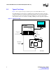
Intel® LXD972M Transceiver Demo Board (Board Rev A1) 2.2 Typical Test Setup Figure 1 shows a typical test setup for standard operation of the LXD972M Demo Board. The LXD972M Demo Board plugs into a SmartBits Advanced Performance Test Box through a standard 40-pin MII cable (not included with the LXD972M Demo Board). The LXD972M Demo Board RJ-45 jack connects to the RJ-45 card in the SmartBits test box through a Twisted-Pair cable.
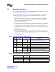
Intel® LXD972M Transceiver Demo Board (Board Rev A1) 2.3 Quick-Start Checklists Use the quick-start checklists in this section to set up the LXD972M Demo Board, shown in Figure 2, “Intel® LXD972M Transceiver Demo Board” on page 10. The following quick-start setup procedure sets all ports to the default condition, which includes Auto-Negotiation enabled, advertising dual-speed, and full-duplex/half-duplex capabilities. 1. Set the jumpers as listed in Table 2.
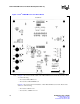
Intel® LXD972M Transceiver Demo Board (Board Rev A1) Figure 2. Intel® LXD972M Transceiver Demo Board SILKSCREEN TOP BOARD ID SERIAL # B3798-001 Note: In Figure 2, the format of the Board ID on the LXD972M Transceiver Demo Board can be either one of the following: • For leaded: LXD972M Rev.A1 • For lead-free: LXD972MLF Rev.
Intel® LXD972M Transceiver Demo Board (Board Rev A1) 2.4 Configurations 2.4.1 Optional Test Setup, Using Two Intel® LXD972M Demo Boards Figure 3 shows an optional test setup using two LXD972M Demo Boards. Each Demo Board plugs into a SmartBits Advanced Performance Test Box through standard 40-pin MII cables. The two LXD972M Demo Boards are linked through a Twisted-Pair crossover cable connected to the RJ-45 jack on each board.
Intel® LXD972M Transceiver Demo Board (Board Rev A1) 2.4.2 Power Supply Voltage Source and Clock Options Table 4 lists banana lead power connectors (BNn) for the LXD972M Demo Board. For details on the power supplies, see the schematic in Chapter 3.0, “Intel® LXD972M Demo Board Schematics”. Table 4. Power Supply Voltage Source Connector Options Reference Designators Signal BN1 VCC BN2 GND BN3 VCCIO BN4 VCCD Supply Description +3.3V.
Intel® LXD972M Transceiver Demo Board (Board Rev A1) Table 7 lists clock configuration options. Table 7. Clock Configuration Options Desired Configuration JP18 Settings Pins 11, 2 Enable Crystal Oscillator Y1 Open Remove jumper from pins 1 and 2 to disable the clock oscillator Y2 output. Jumper Place a jumper on pins 3 and 4 and pins 5 and 6, which connects a crystal across XI and XO to enable Y1. Jumper Place a jumper on pins 1 and 2, which enables the output of clock oscillator Y2.
Intel® LXD972M Transceiver Demo Board (Board Rev A1) 2.4.5 CFG Pin Configuration Options Three control jumpers pull the associated port configuration pins High or Low to select the desired mode (auto-negotiation, speed, and duplex). When auto-negotiation is enabled with LED/CFG1 (JP1) = 1, then LED/CFG2 (JP2), and LED/CFG3 (JP3) are used to configure default advertising characteristics of the LXD972M Demo Board. The desired modes and jumper configuration settings are listed in Table 9.
Intel® LXD972M Transceiver Demo Board (Board Rev A1) Intel® LXD972M Demo Board Schematics 3.
1 2 3 4 S2 A GND LXT972M: 3.3V LXT972M: 2.5V/3.3V 1 BN2 BN4 VCCD BN3 1 1 1 VCCIO BN1 1 + 74LVX14 U5A VCC C31 R67 10K 10uF GND + VCC LXT972M: 3.
1 2 3 A GND 21 22 23 24 25 26 27 28 29 30 31 32 33 34 35 36 37 38 39 40 MII 40 PIN P1 1 2 3 4 5 6 7 8 9 10 11 12 13 14 15 16 17 18 19 20 R40 R41 R42 R43 R44 B C15 0.
1 2 3 TPFON TPFOP TPFIN TPFIP DTP1 + A DIFF TP + DIFF TP 270pF C44 GND C17 0.01uF 270pF C43 DTP2 50 1% R5 50 1% R4 VCCA B TX CT VOLTAGE SET JUMPER 1X1 JP4 FB5 FERRITE GND C49 0.01uF C 0.001uF 2KV C59 0.001uF 2KV C58 8 7 10 9 6 11 3 2 15 14 1 16 Halo TG110-S050N5 T1 TP PORT C C47 0.001uF 2KV C48 0.001uF 2KV D 50 1% R9 DTP3 R13 50 1% 50 1% R8 C18 0.
Document Number: 303125 Revision Number: 002 Revision Date: October 22, 2004 1 2 3 4 A XIN GND C37 20pF 0 R74 TP37 1 Preliminary User’s Guide GND C50 0.1uF GND R76 50 1% R75 X C16 0.
Intel® LXD972M Transceiver Demo Board (Board Rev A1) 4.0 Bill of Materials Table 11 lists the bill of materials for the LXD972M Demo Board Rev A1. Table 11. Bill of Materials (Sheet 1 of 3) 20 Board Reference Designator Description Manufacturer Part Number Quantity BN1-4 CONN BANANA NUT SILVER (BANANA_NUT) EF JOHNSON 108-0740-001 4 C1, C2, C5, C8, C9, C11, C13, C38-C42, C45, C46 LABELS NOT USED IN SCHEMATIC.
Intel® LXD972M Transceiver Demo Board (Board Rev A1) Table 11. Bill of Materials (Sheet 2 of 3) Board Reference Designator Description JP5-JP11, JP13, JP15 LABELS NOT USED IN SCHEMATIC.
Intel® LXD972M Transceiver Demo Board (Board Rev A1) Table 11. Bill of Materials (Sheet 3 of 3) 22 Board Reference Designator Description TP1, TP6-14, TP23, TP31-33 LABELS NOT USED IN SCHEMATIC. U1, U3 IC LOGIC 74LVC244 LOW VOLTAGE BUFFER 20 PIN SOIC TEXAS INSTRUMENTS SN74LVC244ADW 2 U2 IC PHY LXT977/LXT972M DUAL PORT (LQFP48C) INTEL LXT977/LXT972M 1 U4 LABELS NOT USED IN SCHEMATIC. U5 IC LOGIC 74LVX14 HEX SCHMITT TRIG INV 14 PIN SOIC TOSHIBA TC74LVX14FN 1 Y1 CRYSTAL 25.