HS-2601A Intel Low Power Mobile 500MHz Mini Board Computer •3.
C Cooppyyrriigghhtt D Diissccllaaiim meerrss The accuracy of contents in this manual has passed thorough checking and review before publishing. BOSER Technology Co., Ltd., the manufacturer and publisher, is not liable for any infringements of patents or other rights resulting from its use. The manufacturer will not be responsible for any direct, indirect, special, incidental or consequential damages arising from the use of this product or documentation, even if advised of the possibility of such damage(s).
Table of Contents Chapter 1 General Description ---------------------------------6 1.1 Major Features ------------------------------------------------------ 2 1.2 Specifications ------------------------------------------------------- 3 1.3 Board Dimensions ------------------------------------------------- 4 Chapter 2 Unpacking ---------------------------------------------5 2.1 Opening the Delivery Package --------------------------------- 5 2.
3.17 Power Connectors ----------------------------------------------- 18 CN1: 4-pin Power Connector ----------------------18 CN5: 2-pin Power Input Connector----------------19 3.18 Keyboard/Mouse Connectors -------------------------------- 19 CN8: 6-pin Keyboard/Mouse Connector ---------19 CN7: PS/2 6-pin Mini DIN Keyboard/Mouse Connector-------------------------------------------19 3.
SSaaffeettyy IInnssttrruuccttiioonnss Integrated circuits on computer boards are sensitive to static electricity. To avoid damaging chips from electrostatic discharge, observe the following precautions: Do not remove boards or integrated circuits from their anti-static packaging until you are ready to install them. Before handling a board or integrated circuit, touch an unpainted portion of the system unit chassis for a few seconds. This helps to discharge any static electricity on your body.
This page intentionally left blank.
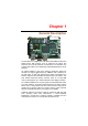
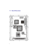
Chapter 1 General Description The HS-2601A is a 100MHz Intel® BX chipset-based Mini PCI Bus Intel Mobile board. With features such as enhanced I/O effects with CRT/VGA, and LAN all combined, the HS-2601A is an ideal all-in-one compact-size board for the demanding embedded applications and IA platforms. Its onboard DMA33 to IDE drive interface architecture allows the HS-2601A to support data transfers of 33MB/sec with a maximum of two IDE drives.
To ensure the reliability in an unmanned or standalone system, the Watchdog Timer (WDT) onboard HS-2601A is designed with pure hardware that does not need the arithmetical functions of a real-time clock chip. If any program causes unexpected halts to the system, the onboard Watchdog Timer (WDT) will automatically reset the CPU or generate an interrupt to resolve such condition. 1.
1.
1.
Chapter 2 Unpacking 2.1 Opening the Delivery Package The HS-2601A is packed in an anti-static bag. The board has components that are easily damaged by static electricity. Do not remove the anti-static wrapping until proper precautions have been taken. Safety Instructions in front of this manual describe anti-static precautions and procedures. 2.2 Inspection After unpacking the board, place it on a raised surface and carefully inspect the board for any damage that might have occurred during shipment.
It is recommended that you keep all the parts of the delivery package intact and store them in a safe/dry place for any unforeseen event requiring the return shipment of the product. In case you discover any missing and/or damaged items from the list of items, please contact your dealer immediately.
Chapter 3 Hardware Installation This chapter provides the information on how to install the hardware using the HS-2601A. This chapter also contains information related to jumper settings of switch, watchdog timer, and the DiskOnChip address selection etc. 3.1 Before Installation After confirming your package contents, you are now ready to install your hardware. The following are important reminders and steps to take before you begin with your installation process. 1.
3.
3.3 Jumper List Jumper JP1 JP2 JP4 3.
3.6 System Memory The HS-2601A provides one SO-DIMM socket at location U2. This onboard memory socket can support 64MB, 128MB and 256MB SO-DIMM modules. The system’s maximum memory capacity is 256MB. 143 1 144 2 144-pin SO-DIMM Socket pin orientation NOTE: 3.7 SO-DIMM sockets out on the market these days have very fragile contacts that attach to modules. We highly recommend you not to regularly remove the installed SO-DIMM from its socket.
3. Once you have figured out where the pin 1 locations are on both chip and socket, align the module’s pins on an upright angle against the socket. Using both thumbs, gently press the module into the socket until all the pins are secured to their designations. Disk OnC hip Pin 1 Location 4. The installation is now complete and your module is now ready for use.
3.8 VGA Controller The HS-2601A has an onboard jumper that selects the working voltage of the flat panel connected to the system. Jumper JP2 offers two voltage settings for the user. JP2: Panel Voltage Select Options Settings 5.0 V (default) 3.3 V Short 1-2 Short 2-3 3 2 1 WARNING: Please contact the supplier of your panel and make sure of the correct voltage it uses. Incorrect settings on JP8 may cause internal damage to your panel.
CN10: 50-pin Panel Connector PIN. Description PIN Description 1 3 5 7 9 11 13 15 17 19 21 23 25 27 29 31 33 35 37 39 41 43 45 47 49 +12V GND Note 3.
3.9 IDE Drive Connector CN12, a 44-pin connector, provides the PCI E-IDE drive provisions onboard. A maximum of four IDE drives may be connected on them.
3.10 Floppy Disk Drive Connector The HS-2601A uses a standard 34-pin header connector, CN11, for floppy disk drive connection. A total of two FDD drives may be connected to CN11 at any given time.
3.11 Serial Port Connectors The HS-2601A offers two NS16C550 compatible UARTs with Read/Receive 16byte FIFO serial ports and two internal 10-pin headers. CN15 and CN14: COM1/COM2 Connector (5x2 Header) PIN Description PIN Description 1 3 5 7 9 DCD RXD TXD DTR GND 2 4 6 8 10 DSR RTX CTX RI N/C DSR 2 1 DCD RTX 4 3 RXD CTX 6 5 TXD RI 8 7 DTR N/C 10 9 GND CN14 and CN15 3.
STBJ PD1 PD3 PD5 PD7 BUSY SLCT ERRJ SUNJ GND GND GND GND 25 1 26 2 PD0 PD2 PD4 PD6 ACKJ PE AFDJ INITJ GND GND GND GND GND 3.13 Ethernet Connector The HS-2601A provides one external RJ-45 10/100 Base-TX LAN interface connector. Please refer to the following detail of pin information.
3.15 USB Connector The HS-2601A provides one 8-pin connector for USB0 & USB1 port connections at location CN13. GND BD1+ 2 8 1 7 GND VCC BD1BD1+ GND BD0+ Description 2 4 6 8 BD0- PIN VCC BD0BD0+ GND VCC Description 1 3 5 7 VCC PIN BD1- CN13: USB Connector 3.16 CMOS Data Clear The HS-2601A has a Clear CMOS jumper on JP4. The JP4 settings below apply to the standard HS-2601A using a battery backed up CMOS chip.
CN5: 2-pin Power Input Connector PIN Description 1 2 +5V GND 1 2 3.18 Keyboard/Mouse Connectors The HS-2601A offers two possibilities for keyboard connections. The connections are via CN7 for an external PS/2 type keyboard/mouse or via CN8 for an internal 5-pin cable converter to an AT keyboard.
LD1 and JP3 are the Keylock and Reset Button connectors onboard. LD1: Power LED PIN Description 1 2 +5V GND 2 1 Description 1 2 GND External Reset 1 2 Ext. Reset PIN GND JP3: Reset Button Connector 3.20 Watchdog Timer There are three access cycles of Watch-Dog Timer as Enable, Refresh and Disable are the three access cycles of Watchdog Timer. The Enable cycle proceeds via READ PORT 443H whereas the Disable cycle proceeds via READ PORT 045H.
After an Enable cycle of WDT, user must immediately execute a Refresh cycle to WDT before its period setting comes to an end every 1, 2, 10, 20, 110 or 220 seconds. If the Refresh cycle does not activate before WDT period cycle, the onboard WDT architecture will issue a Reset or NMI cycle to the system. There are three I/O ports that control the Watchdog Timer.
3.21 CompactFlash Connector Si de Fa Ma br de iq in ue J Au apa Ja n / po n Re ar CE CF C om pa ct Fl as hT M PC Si B de So Vi lde ew r The HS-2601A also offers an optional CompactFlash connector which is IDE interface located at the solder side of the board (beneath the SO-DIMM connector). The designated CN17 connector, once soldered with an adapter, can hold CompactFlash cards of various sizes. Please turn off the power before inserting the CF card.
3.22 Mini PCI Connector HS-2601A supports a Mini PCI interface which is a very popular notebook computer expansion interface for Modem, Video, LAN, etc. The Mini PCI onboard HS-2601A is at location PC1 with pin definitions listed on the table below. PC1: Mini PCI Connector Pin Information PIN. Description PIN. Description 1 3 5 7 9 11 13 15 17 19 21 23 25 27 29 31 33 35 37 39 41 43 45 47 49 51 53 55 57 59 61 63 65 67 69 INTB# 3.3V RESERVED GND CLK GND REQ# 3.
PIN. Description PIN. Description 71 73 75 77 79 81 83 85 87 89 91 93 95 97 99 AD[7] 3.3V AD[5] RESERVED AD[3] 5V AD[1] GND AC_SYNC AC_SDATA_IN AC_BIT_CLK AC_CODEC_ID1# MOD_AUDIO_MON AUDIO_GND SYS_AUDIO_OUT 72 74 76 78 80 82 84 86 88 90 92 94 96 98 100 3.
3.23 PC/104 Connectors The PC/104 expansion bus offers provisions to connect all types of PC/104 modules. With the PC/104 bus being known as the new generation of industrial embedded 16bit PC standard bus, thousands of PC/104 modules from multiple venders can be easily installed onboard.
CN2: 64-pin PC/104 Expansion Slot PIN 1 2 3 4 5 6 7 8 9 10 11 12 13 14 15 16 17 18 19 20 21 22 23 24 25 26 27 28 29 30 31 32 26 Description PIN Description IOCHECK* SD7 SD6 SD5 SD4 SD3 SD2 SD1 SD0 IOCHRDY AEN SA19 SA18 SA17 SA16 SA15 SA14 SA13 SA12 SA11 SA10 SA9 SA8 SA7 SA6 SA5 SA4 SA3 SA2 SA1 SA0 GND 33 34 35 36 37 38 39 40 41 42 43 44 45 46 47 48 49 50 51 52 53 54 55 56 57 58 59 60 61 62 63 64 GND RESETDRV +5V IRQ9 -5V DRQ2 -12V NOW* +12V GND SMEMW* SMEMR* IOW* IOR* DACK3* DRQ3 DACK1* DRQ1 REFRESH* SY
Chapter 4 Award BIOS Setup The HS-2601A uses Award PCI/ISA BIOS for the system configuration. The Award BIOS setup program is designed to provide the maximum flexibility in configuring the system by offering various options that could be selected for end-user requirements. This chapter is written to assist you in the proper usage of these features. 4.1 Starting Setup The Award BIOS is immediately activated when you first power on the computer.
4.2 Using Setup In general, you use the arrow keys to highlight items, press to select, use the and keys to change entries, press for help and press to quit. The following table provides more detail about how to navigate in the Setup program using the keyboard.
4.3 Main Menu Once you enter the Award BIOS CMOS Setup Utility, the Main Menu will appear on the screen. The Main Menu allows you to select from several setup functions and two exit choices. Use the arrow keys to select among the items and press to enter the sub-menu. ROM PCI/ISA BIOS (2A69KD2L) CMOS SETUP UTILITY AWARD SOFTWARE, INC.
Load Setup Defaults The chipset defaults are settings that provide for maximum system performance. While Award has designed the custom BIOS to maximize performance, the manufacturer has the right to change these defaults to meet their needs. Integrated Peripherals This section page includes all the items of IDE hard drive and Programmed Input / Output features. Set Supervisor / User Password Change, set, or disable password. It allows you to limit access to the system and Setup, or just to Setup.
4.4 Standard CMOS Setup The Standard Setup is used for the basic hardware system configuration. The main function is for Data/Time and Floppy/Hard Disk Drive settings. Please refer to the following screen for the setup. When the IDE hard disk drive you are using is larger than 528MB, you must set the HDD mode to LBA mode. Please use the IDE Setup Utility in BIOS SETUP to install the HDD correctly. ROM PCI/ISA BIOS (2A69KD2L) STANDARD CMOS SETUP AWARD SOFTWARE, INC.
Primary Master/Slave & Secondary Master/Slave Drives: The categories identify the types of 4 channels that have been installed in the computer. There are 45 predefined types with 4 user-definable types for Enhanced IDE BIOS. Type 1 to Type 45 are predefined. Type user is user-definable. Press PgUp or PgDn to select a numbered hard disk type or type the number and press . Note that the specifications of your drive must match with the drive table.
LCD&CRT: The category selects the type of video adapter used for the system monitor. Although secondary monitors are supported, you do not have to select the type in Setup. BOTH LCD CRT Auto Enables display of both CRT and LCD Enables display of LCD displays only Enables display of CRT displays only Auto detects the installed display on the system Halt On: The category determines whether the computer will stop if an error is detected during power up.
4.5 BIOS Features Setup This section allows you to configure your system for the basic operation. You have the opportunity to select the system’s default speed, boot-up sequence, keyboard operation, shadowing and security. ROM PCI/ISA BIOS (2A69KD2L) BIOS FEATURES SETUP AWARD SOFTWARE, INC.
NOTE: Many disk diagnostic programs that attempt to access the boot sector table can cause the above warning message. If you will be running such a program, we recommend that you first disable Virus Protection beforehand. CPU Internal Cache/External Cache: These two categories speed up memory access. However, it depends on CPU/chipset design. The default value is en able.
Boot Up Floppy Seek: During POST, BIOS will determine if the floppy disk drive installed is 40 or 80 tracks. 360K type is 40 tracks while 760K, 1.2M and 1.44M are all 80 tracks. Enabled Disabled BIOS searches for floppy disk drive to determine if it is 40 or 80 tracks. Note that BIOS cannot tell from 720K, 1.2M or 1.44M drive type as they are all 80 tracks. BIOS will not search for the type of floppy disk drive by track number.
Typematic Rate (Chars/Sec): When the typematic rate is enabled, this selection allows you select the rate at which the keys are accelerated.
Report No FDD For WIN 95: Whether report no FDD for Win 95 or not. The available choices are Yes, No. Video BIOS Shadow: Determines whether video BIOS will be copied to RAM. However, it is optional depending on chipset design. Video Shadow will increase the video speed. Enabled Disabled Video shadow is enabled Video shadow is disabled C8000 - CBFFF Shadow/D0000 - DFFFF Shadow: These categories determine whether option ROMs will be copied to RAM.
4.6 Chipset Features Setup This section allows you to configure the system based on the specific features of the installed chipset. This chipset manages bus speeds and the access to the system memory resources, such as DRAM and the external cache. It also coordinates the communications between the conventional ISA and PCI buses. It must be stated that these items should never be altered. The default settings have been chosen because they provide the best operating conditions for your system.
50ns 60ns DRAM Timing Type DRAM Timing Type EDO CASx# MA Wait State: You could select the timing control type of EDO DRAM CAS MA (memory address bus). The available choices are 1, 2. EDO RASx# Wait State: You could select the timing control type of EDO DRAM RAS MA (memory address bus). The available choices are 1, 2. SDRAM RAS to CAS Delay: You can select RAS to CAS Delay time in HCLKs of 2/2 or 3/3. The system board designer should set the values in this field, depending on the DRAM installed.
Enabled Disabled Video BIOS access cached Video BIOS access not cached Video RAM Cacheable: Select Enabled allows caching of the video RAM , resulting in better system performance. However, if any program writes to this memory area, a system error may result. 8 Bit I/O Recovery Time: The recovery time is the length of time, measured in CPU clocks, which the system will delay after the completion of an input/output request.
Power-Supply Type: This item allows you to select the type of power supply installed to your board. The available choices are Auto (for auto-detection), P8&P9 (for AT power supplies), and ATX (for ATX power supply). Auto Detect DIMM/PCI Clk: This item allows you to enable/disable auto detect DIMM/PCI Clock. The available choices are Enabled, Disabled. Spread Spectrum: When the system clock generator pulses, the extreme values of the pulse generate excess EMI.
4.7 Power Management Setup The Power Management Setup allows user to configure the system for saving energy in a most effective way while operating in a manner consistent with his own style of computer use. ROM PCI/ISA BIOS (2A69KD2L) POWER MANAGEMENT SETUP AWARD SOFTWARE, INC.
Power Management: This category allows you to select the type (or degree) of power saving and is directly related to the following modes: Doze Mode Standby Mode Suspend Mode HDD Power Down There are four selections for Power Management, three of which have fixed mode settings. Disable (default) Min. Power Saving Max. Power Saving User Defined No power management. Disables all four modes Minimum power management. Doze Mode = 1 hr. Standby Mode = 1 hr., Suspend Mode = 1 hr., and HDD Power Down = 15 min.
MODEM Use IRQ: This item determines the IRQ in which the MODEM can be used. The available choices are 3, 4, 5, 7, 9, 10, 11, NA. 4.7.1 PM Timers The following four modes are Green PC power saving functions that are only user configurable when User Defined Power Management has been selected. See above for available selections. Doze Mode: When enabled and after the set time of system inactivity, the CPU clock will run at slower speed while all other devices still operate at full speed.
PowerOn by Ring: An input signal on the serial Ring Indicator (RI) line (in other words, an incoming call on the modem) awakens the system from a soft off state. The available choices are Enabled, Disabled. Wake Up On LAN: An input signal on the local area network (LAN) awakens the system from a soft off state. IRQ 8 Break Suspend: You can Enable or Disable monitoring of IRQ8 so it does not awaken the system from Suspend mode. The available choices are Enabled, Disabled. 4.7.
4.8 PNP/PCI Configuration This section describes configuring the PCI bus system. PCI, or Personal Computer Interconnect, is a system that allows I/O devices to operate at speeds nearing the speed the CPU itself uses when communicating with its own special components. This section covers some very technical items and it is strongly recommended that only experienced users should make any changes to the default settings. ROM PCI/ISA BIOS (2A69KD2L) PNP/PCI CONFIGURATION AWARD SOFTWARE, INC.
Assign IRQ For VGA/USB: This option turns on or off the IRQ assignment for both VGA and USB ports. 4.9 Load BIOS Defaults When you press on this item you will get a confirmation dialog box with a message shown below. This option allows you to load/restore the BIOS default values permanently stored in the BIOS ROM. Pressing ‘Y’ loads the BIOS default values for the most stable, minimal-performance system operations. ROM PCI/ISA BIOS (2A69KD2L) LOAD BIOS DEFAULTS AWARD SOFTWARE, INC.
4.10 Load Setup Defaults When you press on this item you get a confirmation dialog box with a message similar to the figure below. This option allows you to load/restore the default values to your system configuration, optimizing and enabling all high performance features. Pressing ‘Y’ loads the default values that are factory settings for optimal performance system operations. ROM PCI/ISA BIOS (2A69KD2L) LOAD SETUP DEFAULTS AWARD SOFTWARE, INC.
4.11 Integrated Peripherals The IDE hard drive controllers can support up to two separate hard drives. These drives have a master/slave relationship that is determined by the cabling configuration used to attach them to the controller. Your system supports two IDE controllers--a primary and a secondary--so you can install up to four separate hard disks. PIO means Programmed Input/Output.
On-Chip Primary/Secondary PCI IDE: The integrated peripheral controller contains an IDE interface that supports a single IDE channels. Select Enabled to activate the channel. USB Keyboard Support: Select Enabled if your system contains a Universal Serial Bus (USB) controller and you have a USB keyboard. The available choices are Enabled, Disabled. Init Display First: This item allows you to decide to active whether PCI Slot or on-chip VGA first The available choices are PCI Slot, Onboard .
IR Transmission delay: Full duplex mode permits simultaneous bi-directional transmission. Half duplex mode permits transmission in one direction only at a time. Select Disabled if there is no infrared port present. Onboard Parallel Port: Select a logical LPT port name and matching address for the physical parallel (printer) port. The available choices are 378H/IRQ7, 278H/IRQ5, 3BCH/IRQ7, Disabled. Parallel Port Mode: Select an operating mode for the onboard parallel port.
4.12 Supervisor/User Password Setting ROM PCI/ISA BIOS (2A69KD2L) CMOS SETUP UTILITY AWARD SOFTWARE, INC.
When a password has been enabled, you will be prompted to enter it every time you try to enter Setup. This prevents an unauthorized person from changing any part of your system configuration. Additionally, when a password is enabled, you can also require the BIOS to request a password every time your system is rebooted. This would prevent unauthorized use of your computer. You determine when the password is required within the BIOS Features Setup Menu and its Security option (see Section 3).
4.14 Save & Exit Setup Pressing on this item asks for confirmation: Pressing “Y” stores the selections made in the menus in CMOS – a special section of memory that stays on after you turn your system off. The next time you boot your computer, the BIOS configures your system according to the Setup selections stored in CMOS. After saving the values the system is restarted again. ROM PCI/ISA BIOS (2A69KD2L) CMOS SETUP UTILITY AWARD SOFTWARE, INC.
4.15 Exit Without Saving Pressing on this item asks for confirmation: Quit without saving (Y/N)? Y This allows you to exit Setup without storing in CMOS any change. The previous selections remain in effect. This exits the Setup utility and restarts your computer. ROM PCI/ISA BIOS (2A69KD2L) CMOS SETUP UTILITY AWARD SOFTWARE, INC.
Chapter 5 Software Utilities This chapter contains the detailed information of IDE, VGA, Audio and LAN driver installation procedures. 5.1 VGA Driver Installation for Win 95/98 1. Click Start, then Setting, then Control Panel. 2. Start the Display applet program.
3. Select the setting page, click on the Advanced properties button. 4. Press the Change button in the adapter area. 5. Click on Next to continue and then select Display a list of all drivers in a specific location, so you can select the drivers you want. 6. Click on Next. 7. Select the Specify a location checkbox then Browse. 8. Specify the path to the new driver and then press the key (if in driver A: select a:\win95). 9. Once completed, the Select device dialog box will appear.
11. After the system has restarted, you can go back into the display applet and select alternate screen resolutions and color depths. NOTE: 5.2 Installation procedure for Windows 98 is similar to Windows95. VGA Driver Installation for Win NT4.0 1. Click the Start button, then go to Settings and click on Control Panel. 2. Click on Display icon to start the Display Properties window. 3. Click on the Settings tab, and then click on Display Type.
4. In the Change Display Type window, click on Have Disk. 5. Specify the path to the new driver and press the key (if in driver A:, type a:\nt40). Select Chips Video Accelerator (655545/48/50/54/55/68554 69000) 6. Click OK or press Enter. 7. You will then see warning panel about Third Party Drivers. Click on Yes to complete installation. 8. Once the installation is complete, the system must be shut down and restarted for the new driver to take effect.
9. After restarting, check on the VGA driver and make sure the properties of the driver look similar to the following figure.
5.3 LAN Driver Installation for WIN95 & WIN98 5.3.1 Win98 Windows 98 will detect the network driver automatically therefore there is no need for further configuration. 5.3.2 Win95 1. Click Start, then Setting then select Control panel. 2. Start the network applet program. 3. In the Network window, click Add. 4. From the Select Network Component Type, select Adapter then click Add.
5. Specify the path the new driver and press key (if in driver a:, type a:\). If you’re not sure exactly where the drivers are, choose the Browse button and find it. 6. Click OK. 7. Windows 95 will copy the network drivers to the proper directories into your system. 8. Continue choosing OK until asked to restart your system. 9. After restarting your computer, check the network driver and its properties. Be sure it looks similar with the following figure.
5.4 LAN Driver Installation for Win NT4.0 1. Click the Start button, then go to Setting and click on Control Panel. 2. Click on the Network icon to start the Network Window. 3. Click on the Adapters tab, and then click Add. 4. In the Select Network Adapter window, click Have Disk. 5. This will bring up the Insert Disk window. 6. Supply the directory where the Windows NT driver files are located (If in driver a: type a:\). 7. The Select OEM Option window will show up.
9. Once the installation is completed, the system must be shut down and restarted for the new driver to take effect. 10. After restart, confirm the network driver and its properties.
This page intentionally left blank.