Intel® 31244 PCI-X to Serial ATA Controller Design Guide April 2004 Order Number: 273651-003
Intel® 31244 PCI-X to Serial ATA Controller INFORMATION IN THIS DOCUMENT IS PROVIDED IN CONNECTION WITH INTELR PRODUCTS.
Intel® 31244 PCI-X to Serial ATA Controller Contents Contents 1 About This Document ......................................................................................................................9 1.1 1.2 2 Overview........................................................................................................................................ 13 2.1 2.2 3 3.2 3.3 4.5 Serial ROM Interface ...................................................................................................
Intel® 31244 PCI-X to Serial ATA Controller Contents 7.3 7.4 8 Cables and Connectors ................................................................................................................. 55 8.1 9 Cabling................................................................................................................................ 55 8.1.1 Serial ATA Cable ................................................................................................... 58 Voltage Power Delivery ..........
Intel® 31244 PCI-X to Serial ATA Controller Contents Figures 1 2 3 4 5 6 7 8 9 10 11 12 13 14 15 16 17 18 19 20 21 22 23 24 25 26 27 Intel® 31244 PCI-X to Serial ATA Controller Block Diagram ...................................................... 14 Quad Serial ATA Host Bus Adapter............................................................................................15 Packaging Considerations ..........................................................................................................
Intel® 31244 PCI-X to Serial ATA Controller Contents Tables 1 2 3 4 5 6 7 8 9 10 11 12 13 14 16 15 17 18 19 20 21 22 23 24 25 26 27 28 29 30 31 32 33 35 34 36 37 38 39 40 41 6 Reference Documents .................................................................................................................. 9 Terminology and Definition ........................................................................................................... 9 Serial ATA Signals Pin Descriptions........................
Intel® 31244 PCI-X to Serial ATA Controller Contents Revision History Date Revision # April 2004 003 Description Removed Section 5.4.5, “Spread Spectrum Clocking” on page 35. Removed SSC pin in Table 2, “Terminology and Definition” on page 9. Updated SSCEN pin in Table 5, “Configuration Pin Descriptions” on page 20 and Table 30, “Terminations: Pull-up/Pull-down” on page 65. Removed Section 9.1, “Power Delivery for the Intel® 31244 PCI-X to Serial ATA Controller (TBD)” on page 59.
Intel® 31244 PCI-X to Serial ATA Controller Contents This page intentionally left blank.
1 About This Document 1.1 Reference Documentation For the latest revision and documentation number, contact your Intel representative. Table 1. Reference Documents Document Intel Document Number or Source Intel® Artisea PCI-X to Serial ATA Controller Developer’s Manual 273603 Intel® Artisea PCI-X to Serial ATA Controller Datasheet 273595 ® Intel Packaging Databook 240800 Printed Circuit Board (PCB)Test Methodology User’s Guide, Revision 1.6 298179 http://developer.intel.
Intel® 31244 PCI-X to Serial ATA Controller About This Document Table 2. Terminology and Definition (Sheet 2 of 3) Term Definition Printed circuit board. Layer 1: copper Prepreg Layer 2: GND Core PCB Layer 3: VCC Prepreg Layer 4: copper Example manufacturing process consists of the following steps: • Consists of alternating layers of core and prepreg stacked • The finished PCB is heated and cured.
Intel® 31244 PCI-X to Serial ATA Controller About This Document Table 2. Terminology and Definition (Sheet 3 of 3) Term RxData 10b encoding Jitter Definition Serially encoded 10b data attached to the high-speed serial differential line receiver. The 8B/10B encoding scheme transmits eight bits as a 10-bit code group. This encoding is used with Gigabit Ethernet, Fibre Channel and InfiniBand*. Jitter is a high-frequency, semi-random displacement of a signal from its ideal location.
Intel® 31244 PCI-X to Serial ATA Controller About This Document This page left intentionally blank.
Intel® 31244 PCI-X to Serial ATA Controller Overview 2 Overview This document provides layout information and guidelines for designing platform or add-in board applications with the Intel® 31244 PCI-X to serial ATA controller (GD31244). It is recommended that this document be used as a guideline. Intel recommends employing best-known design practices with board-level simulation, signal integrity testing and validation for a robust design.
Intel® 31244 PCI-X to Serial ATA Controller Overview Feature Highlights: • • • • • • • • • • Figure 1. Four SATA Channels at 1.5 Gbits/s Serial ATA: High speed Serialized AT Attachment Specification, Revision 1.0e Compliant 64-bit/133 MHz PCI-X Bus.
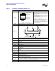
2.2 Applications The GD31244 may be used to build a Serial ATA Host Bus Adapter which connects to the PCI-X bus. Control for external activity LEDs, a 37.5 MHz Crystal, a voltage regulator and some external resistors and capacitors are needed. Quad Serial ATA Host Bus Adapter 3.3V VIO JTAG PCI-X Bus P_AD[63:0] P_CBE[7:0] P_PAR P_PAR64 P_FRAME# P_TRDY# P_IRDY# P_STOP# P_DEVSEL# P_REQ# P_REQ64# P_ACK64# P_GNT# P_CLK P_IDSEL P_RST# P_PERR# P_SERR# P_INTA# 2.
Intel® 31244 PCI-X to Serial ATA Controller Overview This page left intentionally blank.
Intel® 31244 PCI-X to Serial ATA Controller Intel® 31244 PCI-X to Serial ATA Controller Package Intel® 31244 PCI-X to Serial ATA Controller Package 3 The GD31244 signals, are located on a 256-pin Plastic Ball Grid Array (PBGA) package to simplify signal routing and system implementation. For detailed signal descriptions refer to the Intel® 31244 PCI-X to Serial ATA Controller Datasheet. Contact your Intel sales representative to obtain a copy of this document.
Intel® 31244 PCI-X to Serial ATA Controller Intel® 31244 PCI-X to Serial ATA Controller Package 3.1 Signal Pin Descriptions The signal pin descriptions for the GD31244 are provided as a reference. A complete list is also available in the Intel® 31244 PCI-X to Serial ATA Controller Datasheet. Table 3. Serial ATA Signals Pin Descriptions Name Description TX0P, TX0N, TX1P, TX1N, TX2P, TX2N, TX3P, TX3N OUTPUT - Differential High-Speed Outputs: These are the differential serial outputs for each channel.
Intel® 31244 PCI-X to Serial ATA Controller Intel® 31244 PCI-X to Serial ATA Controller Package Table 4. PCI-X Bus Pin Descriptions (Sheet 1 of 2) Name CAP2, CAP3 Analog: An external 0.015 µF (+/- 10%) capacitor is connected between these pins to set the PCI PLL loop filter response. P_ACK64# BIDIRECTIONAL - LVTTL: Indicates that the device has positively decoded its address as the target of the current access and the target is willing to transfer data using the full 64-bit data bus.
Intel® 31244 PCI-X to Serial ATA Controller Intel® 31244 PCI-X to Serial ATA Controller Package Table 4. PCI-X Bus Pin Descriptions (Sheet 2 of 2) Name Description P_REQ64# BIDIRECTIONAL - LVTTL: Indicates the attempt of a 64-bit transaction on the PCI bus. When the target is 64-bit capable, the target acknowledges the attempt with the assertion of P_ACK64#. P_RST# Table 5. Table 6. P_SERR# OUTPUT - Open Drain with Pull-Up Resistor: System Error.
Intel® 31244 PCI-X to Serial ATA Controller Intel® 31244 PCI-X to Serial ATA Controller Package Table 7. Serial ROM Interface Pin Descriptions Name Description SDI INPUT - LVTTL with Pull Up: Connects to the serial data output (SDO) of the Serial ROM. Customers are recommended to add pads for both a pull-up and a pull-down resistor for possible use in the future. SDO (LED3) OUTPUT - LVTTL: Connects to the serial data input (SDI) of the Serial ROM.
Intel® 31244 PCI-X to Serial ATA Controller Intel® 31244 PCI-X to Serial ATA Controller Package 3.2 Package/Marking Information The package is marked with three lines of text as shown in Figure 4. (The figure is not to scale.) Figure 4. Package Information: 256-pin PBGA 16 15 14 13 12 11 10 9 8 7 6 5 4 3 2 1 A B C D E F G H J K L M N P R T Pin A1 Indicator 17mm This page left intentionally blank. 1.0 mm, Typ 17mm 3x 0.50 R BOTTOM VIEW TOP VIEW 2.06 ± 0.
3.3 Ball Map By Function Figure 5 shows the 544 BGA pins mapped by pin function. This diagram is helpful in placing components around the GD31244 for the layout of a PCB. To simplify routing and minimize the number of cross traces, keep this layout in mind when placing components on your board. Name signals, by design, are located on the PBGA package to simplify signal routing and system implementation. Figure 5.
Intel® 31244 PCI-X to Serial ATA Controller Intel® 31244 PCI-X to Serial ATA Controller Package This page left intentionally blank.
Intel® 31244 PCI-X to Serial ATA Controller Routing Guidelines 4 Routing Guidelines This chapter provides routing guidelines for layout and design of a printed circuit board using the GD31244. The high-speed clocking required when designing with the GD31244 requires special attention to signal integrity. In fact, it is highly recommended that the board design be simulated to determine optimum layout for signal integrity.
Intel® 31244 PCI-X to Serial ATA Controller Routing Guidelines 4.2 Crosstalk Crosstalk is caused by capacitive and inductive coupling between signals. Crosstalk is composed of both backward and forward crosstalk components. Backward crosstalk creates an induced signal on victim network that propagates in the opposite direction of the aggressor signal. Forward crosstalk creates a signal that propagates in the same direction as the aggressor signal.
Intel® 31244 PCI-X to Serial ATA Controller Routing Guidelines 4.3 EMI Considerations It is highly recommended that good EMI design practices be followed when designing with the Intel® 31244 PCI-X to serial ATA controller. • To minimize EMI on your PCB a useful technique is to not extend the power planes to the edge of the board. • Another technique is to surround the perimeter of your PCB layers with a GND trace. This helps to shield the PCB with grounds minimizing radiation.
Intel® 31244 PCI-X to Serial ATA Controller Routing Guidelines 4.4 Power Distribution and Decoupling Have ample decoupling to ground, for the power planes, to minimize the effects of the switching currents. Three types of decoupling are: the bulk, the high-frequency ceramic, and the inter-plane capacitors. • Bulk capacitance consist of electrolytic or tantalum capacitors. These capacitors supply large reservoirs of charge, but they are useful only at lower frequencies due to lead inductance effects.
4.5 Trace Impedance All signal layers require controlled impedance of 50 Ω +/- 15%, microstrip or stripline where appropriate, unless otherwise specified. Selecting the appropriate board stack-up to minimize impedance variations is very important. When calculating flight times, it is important to consider the minimum and maximum trace impedance based on the switching neighboring traces. Use wider spaces between traces, since this may minimize trace-to-trace coupling, and reduce cross talk.
Intel® 31244 PCI-X to Serial ATA Controller Routing Guidelines For a symmetric trace Z11 = Z22, the differential impedance may be calculated from this equation: Zdifferential = 2(Z11-Z12) For two traces to be symmetric, they must have the same width, thickness and height above the ground plane.1 With the traces terminated with the appropriate differential, impedance ringing is minimized. 1.
Intel® 31244 PCI-X to Serial ATA Controller Intel® 31244 PCI-X to Serial ATA Controller Interface Ports Intel® 31244 PCI-X to Serial ATA Controller Interface Ports 5.1 5 Serial ROM Interface In add-in card applications, firmware may be downloaded to the system from a Serial EEPROM or Serial Flash ROM, through the Serial ROM Interface. This industry standard, 4-pin interface, allows any size of device, up to 128 Kbytes, to be connected to the Intel® GD31244 PCI-X to serial ATA controller.
Intel® 31244 PCI-X to Serial ATA Controller Intel® 31244 PCI-X to Serial ATA Controller Interface Ports 5.3 PCI-X Interface The 64-bit, 133 MHz PCI-X interface is fully compliant with the PCI Local Bus Specification, Revision 2.2 and the PCI-X Addendum to the PCI Local Bus Specification, Revision 1.0a. The PCI-X bus supports up to 1064 Mbytes/s transfer rate of burst data. The GD31244 is backwards compatible with 32-bit/33 MHz, 32-bit/66 MHz and 64-bit/66 MHz operation.
Intel® 31244 PCI-X to Serial ATA Controller Intel® 31244 PCI-X to Serial ATA Controller Interface Ports 5.4 Serial ATA Interface Four 1.5 Gbits/s Serial ATA ports are located on the GD31244, to support point-to-point connectivity to disk drives, CDROMs, DVD ROMs or any other Serial ATA target device. Each port is compliant with the “Serial ATA: High speed Serialized AT Attachment Specification, Revision 1.0e.
Intel® 31244 PCI-X to Serial ATA Controller Intel® 31244 PCI-X to Serial ATA Controller Interface Ports 5.4.3 LED Interface Serial ATA interfaces on disk drives do not include the traditional ATA output, which drives an LED to indicate that the drive is active. The GD31244 compensates for this missing function by adding four LED outputs, which sink 10 mA. In Master/Slave compatibility mode, LED0 goes LOW to turn on an Activity LED, anytime there is activity on either Channel 0 or Channel 1.
5.4.4 Reference Clock Generation A 37.5 MHz reference clock with a +/- 100 ppm accuracy is required for proper operation of the GD31244. This is generated from an external oscillator connected directly to the XI input. Optionally, a 37.5 MHz crystal may be connected between the XI and XO pins with a 20 pF capacitor from XI to ground and another from XO to ground. The following are the crystal characteristics: • • • • • • • • Frequency: 37.
Intel® 31244 PCI-X to Serial ATA Controller Intel® 31244 PCI-X to Serial ATA Controller Interface Ports This page left intentionally blank.
Intel® 31244 PCI-X to Serial ATA Controller Printed Circuit Board (PCB) Methodology Printed Circuit Board (PCB) Methodology 6 This section provides a recommended guidelines for PCB stackup. A considerable part of the SI analysis, is to identify and recommend the backplane stackup recommendations. This guideline section is separated into two recommendations: • GD31244 in normal mode, refer to Table 9. • GD31244 in extended voltage mode for backplane designs, refer to Table 10.
Intel® 31244 PCI-X to Serial ATA Controller Printed Circuit Board (PCB) Methodology 6.1 Intel® 31244 PCI-X to Serial ATA Controller Normal Mode (standard SATA driver) This section provides recommendations for the GD31244 running in the standard SATA mode. Figure 11 shows a standard SATA setup with the GD31244 connected to trace on the motherboard. This trace terminates with a connector. The SATA cable connects to the SATA motherboard cable with the other end connecting to connector on the hard drive.
Intel® 31244 PCI-X to Serial ATA Controller Printed Circuit Board (PCB) Methodology Intel® 31244 PCI-X to Serial ATA Controller HBA Stackup 6.1.1 The below stackup in Figure 12, shows the layer topology that is used in the HBA customer reference board. The first layer, Layer 0 is a signal layer, the second layer, Layer 1 is ground, the third layer, Layer 2 is 2.5 V plane with some traces, the fourth layer, Layer 3 is the 3.
Intel® 31244 PCI-X to Serial ATA Controller Printed Circuit Board (PCB) Methodology • • • • 6.2.1 Jitter tolerance (TJ) must be >= 0.7 UI vs 0.62 UI of spec (@RCV pin) Slowest edge rate assumed Used only for GD31244 reads Read eye was guardbanded by 10 mV to allow for crosstalk Backplane Topologies This analysis looks at two backplane interconnection topologies. These two backplane topologies are divided into the two categories for the read RX lines and write TX lines.
Intel® 31244 PCI-X to Serial ATA Controller Printed Circuit Board (PCB) Methodology Figure 14. Read Backplane Topology a. Read Backplane Topology Package Model Connector Intel® 31224 MB SD Connector BP MB BP HDD SD b.
Intel® 31244 PCI-X to Serial ATA Controller Printed Circuit Board (PCB) Methodology 6.2.2 Motherboard Stackup for Backplane Designs The motherboard is supporting components in addition to GD31244, so an assumption is, desktop PC requirements are dominate to assure the processor and memory subsystem may be implemented with normal 60 ohm guidelines. Table 12. Table 13. Motherboard Stackup, Microstrip Variable Nominal (mil) Tolerance Min (mil) Max (mil) Mask Thickness 0.8 +/- 0.2 0.6 1.
Figure 15. Microstrip Stackup 5 mil 1.4 mil + 10 mil Mask Er = 3.65 - 0.8 mil + - 55 mil Er = 4.15 4 mil 1.
Intel® 31244 PCI-X to Serial ATA Controller Printed Circuit Board (PCB) Methodology 6.2.3 Backplane Stripline Stackup Figure 16 provides an example stackup that may be used to implement the backplane design. The stripline shown in Figure 16 is implemented with ground flood on both component and solder side of the PCB. The differential stripline traces are etched from the power and ground planes. Note that this information is preliminary. Table 14.
Intel® 31244 PCI-X to Serial ATA Controller Printed Circuit Board (PCB) Methodology Table 15. Backplane Stackup, Microstrip Variable Table 16. 6.2.4 Nominal (mil) Tolerance Mask Thickness 0.8 +/- 0.2 Mask Er 3.6 Trace Height 1.4 Preg Er Min (mil) Max (mil) 0.6 1.0 3.6 3.6 +/-0.3 1.1 1.7 4.66 +/-0.55 3.6 4.7 Plane Thickness 1.4 +/-0.2 1.2 1.6 Trace Thickness 1.4 +/-0.4 1.0 1.8 Trace Width 11.5 +/-1.5 10 13 Total Thickness 70.0 +/-7.0 63.0 77.
Intel® 31244 PCI-X to Serial ATA Controller Printed Circuit Board (PCB) Methodology This page left intentionally blank.
Intel® 31244 PCI-X to Serial ATA Controller PCI-X Layout Guidelines 7 PCI-X Layout Guidelines This section provides guidelines for designing with the Intel® 31244 PCI-X to serial ATA controller PCI/PCI-X (PCI/X) bus interface in your application. This chapter is divided as follows: • • • • 7.
Intel® 31244 PCI-X to Serial ATA Controller PCI-X Layout Guidelines 7.2 PCI/X Clocking Modes The Intel® 31244 PCI-X to serial ATA controller clocking modes for PCI-X and PCI bus are shown in Table 19. At PCI bus reset, the Intel® 80321 I/O processor samples the P_FRAME#, P_IRDY#, P_TRDY#, P_STOP#, and P_DEVSEL# to determine the operating frequency for PCI-X mode. When P_FRAME# is deasserted and P_IRDY# is deasserted (i.e.
Intel® 31244 PCI-X to Serial ATA Controller PCI-X Layout Guidelines 7.3 PCI General Layout Guidelines For acceptable signal integrity with bus speeds up to 133 MHz it is important to PCB design layout have controlled impedance. • Signal traces have an unloaded impedance of 60 +/- 10% Ω. • Signal trace velocity is roughly 150 – 190 ps/inch The below list provides general guidelines used when routing your PCI bus signals: • Avoid routing signals > 8”. • All clock nets must be on the top layer.
Intel® 31244 PCI-X to Serial ATA Controller PCI-X Layout Guidelines 7.4 PCI-X Layout Guidelines For Slot Configurations The PCI-X Addendum to the PCI Local Bus Specification, Revision 1.0a recommends the following guidelines for the number of loads for your PCI-X designs. Any deviation from these maximum values requires close attention to layout with regard to loading and trace lengths. Table 21.
7.4.2 PCI Clock Layout Guidelines The PCI-X Addendum to the PCI Local Bus Specification, Revision 1.0a, allows a maximum of 0.5 ns clock skew timing for each of the PCI-X frequencies: 66 MHz, 100 MHz and 133 MHz. A typical PCI-X application may require separate clock point-to-point connections, distributed to each PCI device. Using a low skew clock buffer helps to meet the maximum clock skew requirements. The clock buffer also provides clock fanout to multiple PCI-X devices.
Intel® 31244 PCI-X to Serial ATA Controller PCI-X Layout Guidelines Connecting Intel® 31244 PCI-X to Serial ATA Controller to Single-Slot 7.4.3 Figure 17 shows one of the chipset PCI AD lines connected through W1 and W12 line segments, to a single-slot connector through W13 line segment, to the GD31244. This AD line is also used as an IDSEL line from line segment W14 to a 2K resistor through W15 to the PCI connector.
Intel® 31244 PCI-X to Serial ATA Controller PCI-X Layout Guidelines 7.4.4 Embedded Intel® 31244 PCI-X to Serial ATA Controller Single PCI-X Load Figure 18 shows GD31244 as the PCI-X agent in a standalone embedded application (with no PCI-X slot). This figure shows one of the chipset PCI AD lines connected through W1 to the Intel® 31244 PCI-X to Serial ATA Controller. This AD line is also used as an IDSEL line from line segment W2 to a 2 K resistor through W3 to the GD31244 IDSEL line input buffer.
Intel® 31244 PCI-X to Serial ATA Controller PCI-X Layout Guidelines 7.4.5 Embedded Intel® 31244 PCI-X to Serial ATA Controller Design With Multiple PCI-X Loads Figure 19 shows GD31244 as the PCI-X agent 1 in a standalone embedded application (with no PCI-X slot) with other PCI-X devices shown as agent 2 and agent 3. This figure shows one of the chipset PCI AD lines connected through W1 to the Intel® 31244 PCI-X to Serial ATA Controller.
8 Cables and Connectors 8.1 Cabling A Serial ATA device is connected to a host through a direct connection or through a cable. For direct connection, the device plug connector, shown as (a) and (b) in Figure 21, is inserted directly into a host receptacle connector, illustrated as (g) in Figure 22. The device plug connector and the host receptacle connector incorporate features that enable the direct connection to be hot pluggable and blind mateable. Table 25.
Intel® 31244 PCI-X to Serial ATA Controller Cables and Connectors For connection through a cable, the device signal plug connector, shown as (a) in Figure 21, mates with the signal cable receptacle connector on one end of the cable, illustrated as (c) in Figure 21.
Figure 22. Serial ATA Host Connectors The signal cable receptacle connector on the other end of the cable is inserted into a host signal plug connector, shown as (f) in Figure 22. The signal cable wire consists of two twinax sections in a common outer sheath. Besides the signal cable, there is also a separate power cable for the cabled connection.
Intel® 31244 PCI-X to Serial ATA Controller Cables and Connectors 8.1.1 Serial ATA Cable The Serial ATA cable consists of four conductors in two differential pairs. When necessary, the cable may also include drain wires, to be terminated to the ground pins in the Serial ATA cable receptacle connectors. The cable size may be 30 to 26 AWG. The cable maximum length is one meter. Figure 23.
Intel® 31244 PCI-X to Serial ATA Controller Voltage Power Delivery Voltage Power Delivery 9 There are two different voltages needed on the Intel® 31244 PCI-X to serial ATA controller. These are VCC of +2.5 V ±5% and VIO of +3.3 V ±10%. Power sequencing is not required on the GD31244. 9.1 Intel® 31244 PCI-X to Serial ATA Controller Core Supply Voltage: Providing 2.5 V in 3.3 V System In most system board designs, the 3.
Intel® 31244 PCI-X to Serial ATA Controller Voltage Power Delivery This page left intentionally blank.
10 Test Methodology The signaling requirements of the SATA specification are measured for signal quality, Table 26 details the values from the SATA Specification, revision 1.0, 29 August 200, starting on page 76. Table 26. Interface Timing and SI Requirements Symbol Min Max Units T,UI Operating data period 666.43 670.12 ps trise 20% to 80% at transmitter 0.2 0.41 UI tfall 80% to 20% at transmitter 0.2 0.
Intel® 31244 PCI-X to Serial ATA Controller Test Methodology The SATA specification defines Figure 24 using values from Table 26 for the legal signaling levels and jitter. Figure 24. Serial ATA Eye Diagram +Vmax V2 +Vmin Illegal Region -Vmin -Vmax T1 T2 T3 T4 T5 T6 T7 T8 B0606-01 Several of oscilloscopes provide eye pattern masking options to allow the user to set up a mask for serial data streams such as Serial ATA.
10.1 Extended Voltage Mode Figure 25, Figure 26, Table 28 and Table 29 describe the extended voltage mode eye diagrams for the modified receiver and driver. These eye diagrams needed to be modified from the original SATA specification to allow for the higher voltage parameters required for a backplane design. Note: 10.1.1 The material in this section is preliminary. Extended Voltage Mode Receiver Model For GD31244 reads, the GD31244 receiver must be more sensitive than the SATA specification.
Intel® 31244 PCI-X to Serial ATA Controller Test Methodology 10.1.2 Extended Voltage Mode Driver Model The extended voltage mode eye diagram for the new slow driver is shown in Figure 26 with the SATA driver mode superimposed. The extended voltage mode eye diagram for the driver is also shown in table format in Table 29. Figure 26. Extended Mode Driver Example 0.3 0.2 Voltage (V) 0.1 0 0 100 200 300 400 500 600 -0.1 old_ideal_S new_ideal_S -0.2 -0.3 Time (ps) B0429-01 Table 29.
Terminations: Pull-down/Pull-ups 11 This chapter provides the requirements for pull-down and pull-up terminations for the Intel® 31244 PCI-X to serial ATA controller. The PCI-X interface pull-down/pull-up recommendation depends on the application. Table 30 details the termination of these signals when the following factors are true: 1. Embedded or motherboard application (non PCI/X plug-in card) with the GD31244 PCI-X interface as the primary interface. 2.
Intel® 31244 PCI-X to Serial ATA Controller Terminations: Pull-down/Pull-ups Table 30. Terminations: Pull-up/Pull-down (Sheet 2 of 2) Signal Name Pull-up or Pull-down TEST0 Connect to GND TOUT NC 32BITPCI# 1K pull-up for 64 bit Controls status bit 16, in the PCI-X Status Register. When pulled down, reports a 0, for a 32-bit bus. When pulled up, reports 1, a 64-bit device. DPA_MODE# GND to enable DPA Mode 1K pull-up to enable legacy mode.
Intel® 31244 PCI-X to Serial ATA Controller Intel® IQ31244 PCI-X to Serial ATA Controller Evaluation Platform Board Intel® IQ31244 PCI-X to Serial ATA Controller Evaluation Platform Board 12 The Intel® IQ31244 PCI-X to Serial ATA Controller Evaluation Platform Board (IQ31244) is an Intel® 80321 I/O processor-based design using a PCI-X bridge, four Intel SATA controllers, and Intel® 82546EB Dual-Port Gigabit Ethernet Controller. The main application for this customer reference board is external storage.
Intel® 31244 PCI-X to Serial ATA Controller Intel® IQ31244 PCI-X to Serial ATA Controller Evaluation Platform Board 12.
Intel® 31244 PCI-X to Serial ATA Controller Debug Connectors and Logic Analyzer Connectivity Debug Connectors and Logic Analyzer Connectivity 13 13.1 Probing PCI-X Signals To ease the probing and debug of the PCI-X signals it is recommended to passively probe the PCI-X bus signals with a logic analyzer.
Intel® 31244 PCI-X to Serial ATA Controller Debug Connectors and Logic Analyzer Connectivity Table 31. Table 32.
Table 33.
Intel® 31244 PCI-X to Serial ATA Controller Debug Connectors and Logic Analyzer Connectivity Table 34. Table 35.
Table 36. Logic Analyzer Pod 6 Mictor-38 Pin Number Even Pod Logic Analyzer Channel Number PCI-X Signal Name 5 CLK/16 Unused 7 15 AD63 9 14 AD62 11 13 AD60 13 12 AD59 15 11 AD58 17 10 AD57 19 9 AD56 21 8 AD55 23 7 AD54 25 6 AD53 27 5 AD52 29 4 AD51 31 3 AD50 33 2 AD49 35 1 AD48 37 0 AD48 The recommended placement of the mictor connectors is at either end of the bus segment.
Intel® 31244 PCI-X to Serial ATA Controller Debug Connectors and Logic Analyzer Connectivity This page left intentionally blank.
Design for Manufacturing 14 The Intel® 31244 PCI-X to Serial ATA Controller is offered in a 256-pin plastic BGA. The construction of this package is shown in Figure 3. PBGA packaging is explained extensively in the Intel® Packaging Databook (Order Number 240800).
Intel® 31244 PCI-X to Serial ATA Controller Design for Manufacturing This page left intentionally blank.
Intel® 31244 PCI-X to Serial ATA Controller Thermal Solutions 15 Thermal Solutions GD31244 is packaged in a 17 mm, 256-pin Plastic Ball Grid Array (PBGA) in an industry-standard footprint. The package includes a four layer substrate with power and ground planes. The construction of the package is shown below. The device is specified for operation when TC (case temperature) is within the range of 0o C to 90o C, depending on the operating conditions. Refer to Figure 3 for a details on the package.
Intel® 31244 PCI-X to Serial ATA Controller Thermal Solutions This page left intentionally blank.
Intel® 31244 PCI-X to Serial ATA Controller References 16 References 16.1 Related Documents The following books and specifications may be helpful for designing with the Intel® 31244 PCI-X to serial ATA controller. Table 39. Design References Design References 1 Transmission Line Design Handbook, Brian C. Wadell 2 Microstrip Lines and Slotlines, K. C. Gupta. Et al. 3 PCI-X Addendum to the PCI Local Bus Specification, Revision 1.0a 4 PCI-X Electrical Subgroup Report, Version1.
Intel® 31244 PCI-X to Serial ATA Controller References 16.2 Electronic Information Table 41. Electronic Information The Intel World-Wide Web (WWW) Location: Customer Support (US and Canada): 80 http://www.intel.
Intel® 31244 PCI-X to Serial ATA Controller Intel® IQ31244 Controller Evaluation Platform Board Bill of Materials Intel® IQ31244 Controller Evaluation Platform Board Bill of Materials A The bill of materials (BOM) identifies all components on the Intel® 31244 PCI-X to Serial ATA Controller HBA reference board. For the most up-to-date BOM, please visit the Intel® website: http://developer.intel.com/design/storage/serialata/docs/gd31244.
Intel® 31244 PCI-X to Serial ATA Controller Intel® IQ31244 Controller Evaluation Platform Board Bill of Materials This page left intentionally blank.