
Datasheet


Intel
®
Itanium
®
Processor 9300 Series and 9500 Series Datasheet 99
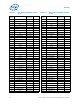
Pin Listing
E34 VCCIO Power/Other
E35 CSI0RPDAT[3] Differential I
E36 VSS Power/Other
E37 CSI0RNDAT[5] Differential I
E38 CSI0RPDAT[5] Differential I
E9 FBD1SBOCP[1] Differential O
F1 RSVD
F2 FBD1SBODN[3] Differential O
F3 FBD1SBODP[3] Differential O
F4 VSS Power/Other
F5 VSS Power/Other
F6 FBD1SBODP[8] Differential O
F7 FBD1SBODN[8] Differential O
F8 VCCIO_FBD Power/Other
F9 VSS Power/Other
F10 FBD1NBICP[11] Differential I
F11 FBD1NBICN[11] Differential I
F12 VSS Power/Other
F13 VSS Power/Other
F14 VSS Power/Other
F15 VSS Power/Other
F16 VCCIO Power/Other
F17 CSI4RNDAT[9] Differential I
F18 CSI4RPDAT[9] Differential I
F19 VSS Power/Other
F20 CSI2RPDAT[3] Differential I
F21 CSI2RNDAT[3] Differential I
F22 VSS Power/Other
F23 VCCIO Power/Other
F24 VSS Power/Other
F25 CSI2TNDAT[2] Differential O
F26 CSI2TNDAT[5] Differential O
F27 CSI2TPDAT[5] Differential O
F28 CSI2TNDAT[8] Differential O
F29 VSS Power/Other
F30 CSI0TNDAT[3] Differential O
F31 CSI0TNDAT[5] Differential O
F32 CSI0TPDAT[5] Differential O
F33 CSI0TNDAT[7] Differential O
F34 VSS Power/Other
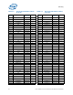
Table 3-2. Pin List by Pin Number (Sheet
21 of 32)
Pin
Number
Pin Name
Signal
Buffer Type
Direction
F35 VCCIO Power/Other
F36 CSI0RNDAT[6] Differential I
F37 CSI0RPDAT[6] Differential I
F38 RSVD
G1 RSVD
G2 VSS Power/Other
G3 FBD1SBODN[1] Differential O
G4 FBD1SBODN[2] Differential O
G5 FBD1SBODP[2] Differential O
G6 FBD1SBODN[10] Differential O
G7 VSS Power/Other
G8 FBD1NBICN[9] Differential I
G9 BOOTMODE[1] I
G10 BOOTMODE[0] I
G11 FBD1NBICN[8] Differential I
G12 VSS Power/Other
G13 VCCIO Power/Other
G14 VSS Power/Other
G15 CSI4TNDAT[4] Differential O
G16 CSI4TPDAT[4] Differential O
G17 VSS Power/Other
G18 CSI4RPCLK Differential I
G19 CSI2RPDAT[2] Differential I
G20 CSI2RNDAT[2] Differential I
G21 CSI2RPDAT[1] Differential I
G22 VSS Power/Other
G23 CSI2TPDAT[0] Differential O
G24 CSI2TNDAT[1] Differential O
G25 CSI2TPDAT[1] Differential O
G26 CSI2TPDAT[4] Differential O
G27 VSS Power/Other
G28 CSI2TPDAT[8] Differential O
G29 VCCIO Power/Other
G30 CSI0TPDAT[2] Differential O
G31 CSI0TNDAT[2] Differential O
G32 VSS Power/Other
G33 CSI0TPDAT[7] Differential O
G34 VCCIO Power/Other
G35 CSI0RNDAT[7] Differential I
G36 CSI0RPDAT[7] Differential I
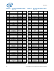
Table 3-2. Pin List by Pin Number (Sheet
22 of 32)
Pin
Number
Pin Name
Signal
Buffer Type
Direction