
Datasheet


Intel
®
Itanium
®
Processor 9300 Series and 9500 Series Datasheet 159
Signal Definitions
7 Signal Definitions
This Chapter provides an alphabetical listing of all Intel
®
Itanium
®
Processor 9300
Series and Intel
®
Itanium
®
Processor 9500 Series signals. The tables list the signal
directions (Input, Output, I/O) and signal descriptions.
For a complete pinout listing including processor specific pins, please refer to
Chapter 3, “Pin Listing”.
Table 7-1. Signal Definitions for the Intel
®
Itanium
®
Processor 9300 Series and Intel
®
Itanium
®
9500 Series (Sheet 1 of 8)
Name Type Description
BOOTMODE[1:0] I The BOOTMODE[1:0] inputs specify which way the Intel
®
Itanium
®
Processor 9300
Series and Intel
®
Itanium
®
Processor 9500 Series will boot. For details on the
modes, refer to the Intel
®
Itanium
®
Processor 9300 Series External Design
Specification or the Intel
®
Itanium
®
Processor 9500 Series External Design
Specification. To pull any of these inputs high, they should be strapped to VCCIO
through a pull-up resistor, and to pull these low, they should be strapped to GND.
These pins are sampled during all resets except warm-logic reset.
CPU_PRES[A|B]_N I/O CPU Present pads. These pins at the top of the package are part of a daisy chain
that indicates to the platform that the processor and Ararat are properly installed
into the socket.
CPU_PRES[1:4]_N I/O CPU Present Pads. These pads at the bottom of the package are part of a daisy
chain that indicates to the platform that the processor and Ararat are properly
installed into the socket. Motherboard routing guidelines for these pins are
documented in the Intel
®
Itanium
®
9300 Series Processor and Intel
®
Itanium
®
Processor 9500 Series Platform Design Guide.
CSI[5:0]R[P/N]CLK I The receive clock signals are inputs to the Intel
®
Itanium
®
Processor 9300 Series
and Intel
®
Itanium
®
9500 Series and are required to be the same frequency at
both ends but may differ by a fixed phase. An Intel
®
QuickPath Interconnect local
receiver port receives a forwarded clock from the transmitter side of the remote
port and vice-versa, to maintain timing reference at either end of the link.
Example: CSI4RPCLK represents port 5 clock receive signal and positive bit of the
differential pair.
CSI[5:0]T[P/N]CLK O These transmit clock signals are driven by the processor and are required to be the
same frequency at both ends but may differ by a fixed phase. An Intel
®
QuickPath
Interconnect local port transmit side sends a forwarded clock to the receive side of
the remote port and vice-versa, to maintain timing reference at either end of the
link.
Example: CSI4TPCLK represents port 5 clock transmit signal and positive bit of the
differential pair.
Intel
®
QuickPath
Interconnect
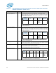
5:0 R P/N CLK0
Interface Name Port
Number
Receiver Differential Pair
Polarity
Positive/
Negative
Clock0
Intel
®
QuickPath
Interconnect
5:0 T P/N CLK0
Interface Name Port Number Transmitter Differential
Pair
Polarity
Positive/
Negative
Clock0