
Guide

Mobile Intel Pentium 4 Processor–M and Mobile Intel Celeron Processor FSB Design Guidelines
R
Intel
®
852GM Chipset Platform Design Guide 31
4. Mobile Intel Pentium 4 Processor–M
and Mobile Intel Celeron Processor
FSB Design Guidelines
The following layout guidelines support designs using the Mobile Intel Pentium 4 Processor–M / Mobile
Intel Celeron Processor and the Intel 852GM chipset. Due to on-die Rtt resistors on both the processor
and the chipset, additional resistors do not need to be placed on the motherboard for most FSB signals.
The exception to these are the RESET# and BPM[5:0]# signals that require a 51.1-Ω pull-up, and the
BR0 signal that requires 220-Ω + 5% pull-up to Vtt on the processor end of the transmission line.
4.1. Processor Front Side Bus (FSB) Routing Guidelines
Table 1 summarizes the layout recommendations for the Mobile Intel Pentium 4 Processor–M and
expands on specific design issues and their recommendations.
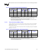
Table 1. Front Side Bus Routing Summary for the Processor
Parameter Processor Routing Guidelines
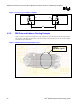
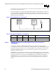
Line to line
spacing
Greater than or equal to 2:1 edge-to-edge spacing versus trace width.
See Figure 3 for an illustration of this recommendation.
Data Line lengths
(agent to agent
spacing)
0.5 inches–5.5 inches from pin-to-pin.
• Data signals of the same source synchronous group should be routed to the same pad-to-pad
length within ± 0.100 inches of the associated strobes.
• The pad is defined as the attach point of the silicon die to the package substrate.
• Length must be added to the system board to compensate for package length differences.
• Signals in the same source synchronous group should be routed on the same layer and
referenced to Vss with 2:1 spacing.
DSTBn/p[3:0]# • A data strobe and its complement should be routed within ± 0.025 inches of the same pad-to-
pad length.
• The pad is defined as the attach point of the silicon die to the package substrate.
• Length must be added to the system board to compensate for package length differences.
• DSTBn/p# should be routed on the same layer as their associated data group and referenced
to Vss.
Address line
lengths (agent to
agent spacing)
0.5 inches – 6.5 inches from pin-to-pin.
• Address signals of the same source synchronous group should be routed to the same Pad-to-
Pad length within± 0.200 inches of the associated strobes.
• The pad is defined as the attach point of the silicon die to the package substrate.
• Length must be added to the system board to compensate for package length differences.
• A layer transition may occur if the reference plane remains the same (Vss) and the layers are
of the same configuration (all stripline or all microstrip).