
Guide

System Memory Design Guidelines (DDR-SDRAM)
R
Intel
®
852GM Chipset Platform Design Guide 83
7. System Memory Design Guidelines
(DDR-SDRAM)
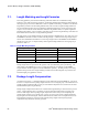
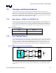
The Intel 852GM GMCH chipset Double Data Rate (DDR) SDRAM system memory interface consists
of SSTL-2 compatible signals. These SSTL-2 compatible signals have been divided into several signal
groups: Data, Control, Command, CPC, Clock, and Feedback signals. Table 30 summarizes the
different signal grouping. Refer to the Intel
®
852GM GMCH Chipset Datasheet for details on the signals
listed.
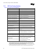
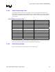
Table 30. Intel 852GM GMCH Chipset DDR Signal Groups
Group Signal Name Description
SCK[4,3,1,0] DDR-SDRAM Differential Clocks - (2 per SO-DIMM)
Clocks
SCK#[4,3,1,0] DDR-SDRAM Inverted Differential Clocks - (2 per SO-DIMM)
SDQ[63:0] Data Bus
SDQS[7:0] Data Strobes
Data
SDM[7:0] Data Mask
SCKE[3:0] Clock Enable - (One per Device Row)
Control
SCS#[3:0] Chip Select - (One per Device Row)
SMA[12:6,3,0] Memory Address Bus
SBA[1:0] Bank Select
SRAS# Row Address Select
SCAS# Column Address Select
Command
SWE# Write Enable
SMA[5,4,2,1] Command per Clock (SO-DIMM0)
CPC
SMAB[5,4,2,1] Command per Clock (SO-DIMM1)
RCVENOUT# Receive Enable Output (no external connection)
Feedback
RCVENIN# Receive Enable Input (no external connection)