
Guide


System Memory Design Guidelines (DDR-SDRAM)
R
Intel
®
852GM Chipset Platform Design Guide 103
7.3.5.3. Control to Clock Length Matching Requirements
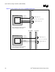
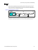
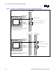
The length of the control signals, between the GMCH die pad and the SO-DIMM must fall within the
range defined below, with respect to the associated clock reference length. Refer to Figure 50 for a
definition of the various trace segments that make up this path. The length of trace from the SO-DIMM
to the termination resistor need not be length matched. The length matching requirements are also
depicted in Figure 51. Refer to Section 7.1 for more details on length matching requirements.
Length range formula for SO-DIMM0:
X
0
= SCK/SCLK#[1:0] total reference length, including package length. See clock Section 7.3.1.
Y
0
= SCS#[1:0] & SCKE[1:0] total length = GMCH package length + L1, as shown in Figure 50,
where: ( X
0
– 1.0” ) ≤ Y
0
≤ ( X
0
+ 0.5” )
Length range formula for SO-DIMM1:
X
1
= SCK/SCLK#[4:3] total reference length, including package length. See clock Section 7.3.1.
Y
1
= SCS#[3:2] & SCKE[3:2] total length = GMCH package length + L1, as shown in Figure 50,
where: ( X
1
– 1.0” ) ≤ Y
1
≤ ( X
1
+ 0.5” )
No length matching is required from the SO-DIMM to the termination resistor. Figure 51 on the
following page depicts the length matching requirements between the control signals and clock. A
nominal CS/CKE package length of 500 mils can be used to estimate baseline MB lengths. Refer to
Section 7.2 for more details on package length compensation.