
Intel Celeron Processor in the 478-Pin Package at 1.80 GHz Datasheet

Datasheet 13
Intel
®
Celeron
®
Processor in the 478-Pin Package
2.0 Electrical Specifications
2.1 System Bus and GTLREF
Celeron processors in the 478-pin package system bus signals use Assisted Gunning Transceiver
Logic (AGTL+) signalling technology. As with the Intel P6 family of microprocessors, this
signalling technology provides improved noise margins and reduced ringing through low voltage
swings and controlled edge rates. Like the Pentium 4 processor, the termination voltage level for
the Celeron
processor in the 478-pin package AGTL+ signals is VCC, which is the operating
voltage of the processor core. The use of a termination voltage that is determined by the processor
core allows better voltage scaling on the system bus for the Celeron
processor in the
478-pin package. Because of the speed improvements to data and address bus, signal integrity and
platform design methods have become more critical than with previous processor families. Design
guidelines for the Celeron
processor in the 478-pin package system bus are detailed in the in the
appropriate Platform Design Guide (refer to Table 1).
The AGTL+ inputs require a reference voltage (GTLREF) which is used by the receivers to
determine if a signal is a logical 0 or a logical 1. GTLREF must be generated on the system board
(see Table 12 for GTLREF specifications). Termination resistors are provided on the processor
silicon and are terminated to its core voltage (V
CC). Intel chipsets will also provide on-die
termination, thus eliminating the need to terminate the bus on the system board for most AGTL+
signals.
Some AGTL+ signals do not include on-die termination and must be terminated on the system
board. See Table 3 for details regarding these signals.
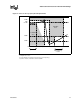
The AGTL+ bus depends on incident wave switching. Therefore timing calculations for AGTL+
signals are based on flight time as opposed to capacitive deratings. Analog signal simulation of the
system bus, including trace lengths, is highly recommended when designing a system.
2.2 Power and Ground Pins
For clean on-chip power distribution, the Celeron
processor in the 478-pin package has 85 VCC
(power) and 181 V
SS (ground) inputs. All power pins must be connected to VCC, while all VSS pins
must be connected to a system ground plane.The processor V
CC pins must be supplied the voltage
determined by the VID (Voltage ID) pins.
2.3 Decoupling Guidelines
Due to its large number of transistors and high internal clock speeds, the processor is capable of
generating large average current swings between low and full power states. This may cause
voltages on power planes to sag below their minimum values if bulk decoupling is not adequate.
Care must be taken in the board design to ensure that the voltage provided to the processor remains
within the specifications listed in Table 6. Failure to do so can result in timing violations or reduced
lifetime of the component. For further information and design guidelines, refer to Table 1 for the
appropriate platform design guide, and the Intel
®
Pentium
®
4 Processor VR-Down Design
Guidelines.