
Guide

Intel Celeron M Processor Front Side Bus Design Guidelines
R
Intel
®
852GM Chipset Platform Design Guide 75
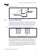
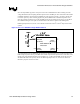
Since the input buffer trip point is set by the 2/3*VCCP on GTLREF and to allow tracking of VCCP
voltage fluctuations, no decoupling should be placed on the GTLREF pin. The node between R1 and R2
(GTLREF) should be connected to the GTLREF pin of the processor with Zo = 55 Ω trace shorter than
0.5 inches. Space any other switching signals away from GTLREF with a minimum separation of 25
mils. Do not allow signal lines to use the GTLREF routing as part of their return path (i.e. do not allow
the GTLREF routing to create splits or discontinuities in the reference planes of the FSB signals).
RSVD signal pins E26, G1, and AC1 are to be left unconnected on Intel
®
Celeron
®
M processor based
systems.
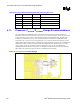
Figure 35. Processor GTLREF Voltage Divider Network
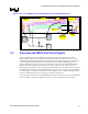
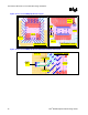
A recommended layout of GTLREF for the processor is shown in Figure 36. To avoid interaction with
FSB routing and power delivery, GTLREF’s R1 and R2 components are placed next to each other on the
primary side of the motherboard and connected with a Zo = 55 Ω to the GTLREF pin on the processor.
The BGA ball lands on the primary side for the RSVD signal pins E26, G1, and AC1 are shown for
illustrative purposes and are not routed.
GTLREF
(pin AD26)
Banias
RSVD
(pin E26)
RSVD
(pin AC1)
RSVD
(pin G1)
GTLREF
R1
1K
1%
R2
2K
1%
+VCCP
< 0.5”
Zo=55
Ω
trace
GTLREF
(pin AD26)
Intel
®
Celeron
®
M
Processor
RSVD
(pin E26)
RSVD
(pin AC1)
RSVD
(pin G1)
GTLREF
R1
1K
1%
R2
2K
1%
+VCCP
< 0.5”
Zo=55
Ω
trace