
Guide

Mobile Intel Pentium 4 Processor–M and Mobile Intel Celeron Processor FSB Design Guidelines
R
36 Intel
®
852GM Chipset Platform Design Guide
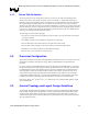
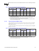
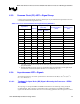
Figure 5. SS Topology for Address and Data
Processor Chip Set
Vtt
Pin
Pad
Pin
Pad
Vtt
L1
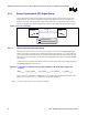
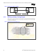
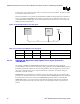
4.3.2. FSB Data and Address Routing Example
Figure 6, Figure 7, Figure 8, and Figure 9 provide examples of a board routing for the Data signal group.
The majority of the Data signal route is on an internal layer; both external layers can be used for parallel
termination R-pack placement.
Figure 6. FSB Host Data Routing Example Layer 3
Layer 3
FSB Data signals