
Intel Celeron Processor for the PGA370 Socket up to 1.40 GHz on 0.13 Micron Process Datasheet

Datasheet 37
Intel
®
Celeron
®
Processor for PGA370 up to 1.40 GHz on 0.13 µ Process
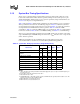
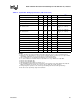
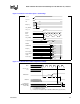
Figure 10. BCLK/BCLK#, PICCLK, and TCK Generic Clock Waveform
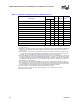
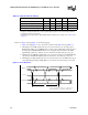
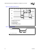
Figure 11. System Bus Valid Delay Timings
V3
V1
V2
T
p
T
l
T
h
T
r
T
f
Vringback
(rise)
Vringback
(fall)
T
r
= T5, T25, T34, (Rise Time)
T
f
= T6, T26, T35, (Fall Time)
T
h
= T3, T23, T32, (High Time)
T
l
= T4, T24, T33, (Low Time)
T
p
= T1, T22, T31 (BCLK, TCK, PICCLK Period)
V1 = BCLK is referenced to 0.30V (Differential Mode), 0.50V (Single-Ended Mode)
TCK is referenced to Vref - 200 mV, PICCLK is referenced to 0.4V.
V2 = BCLK is refernced to 0.9V (Differental Mode), 2.0V (Single-Ended Mode)
TCK is referenced to Vref + 200 mV, PICCLK is refernced to 1.6V
V3 = BCLK and BLCK# crossing point of the rising edge of BLCK and the falling edge of BCLK# (Differential Mode),
BCLK i refereced to 1.25V (Single-Ended Mode), PICCLK is reference to 1.0V, TCK is referenced to Vcmosref
0V
Vih diff
Vil diff
BCLK
Signal
Valid
Tx
V
Tx
Tpw
Tx = T7, T29a, T29b (Valid Delay)
Tpw = T14, T15 (Pulse Width)
V = Vref for AGTL signal group; Vcmosref for CMOS, APIC and TAP signal groups
BCLK#
Valid
NOTE: Single-Ended clock uses BCLK only,
Differential clock uses BCLK and BCLK#