
Intel Celeron Processor for the PGA370 Socket up to 1.40 GHz on 0.13 Micron Process Datasheet

36 Datasheet
Intel
®
Celeron
®
Processor for PGA370 up to 1.40 GHz on 0.13 µ Process
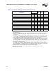
NOTES:
1. All signals, during their invalid states, must be guarded against spurious levels from effecting the platform
during processor power-up sequence.
2. Configuration Input signals include: A[14:5], BR0#, INIT#. For timing of these signals, refer to Table 18 and
Figure 13.
Notes: For Figure 9 through Figure 19, the following apply:
1. Figure 9 through Figure 19 are to be used in conjunction with Table 14 through Table 21.
2. All timings for the AGTL signals at the processor pins are referenced to the rising edge of
BCLK and the falling edge of BCLK# at the crossing point for differential clock mode and to
the rising edge of BCLK at BCLK
VREF
(1.25 V) for single-ended clock mode. All AGTL
signal timings (address bus, data bus, etc.) are referenced at 2/3V
TT at the processor pins.
3. All timings for the APIC I/O signals at the processor pins are referenced to the PICCLK rising
edge at 0.9 V. All APIC I/O signal timings are referenced at 1.0 V at the processor pins.
4. All timings for the TAP signals at the processor pins are referenced to the TCK rising edge at
1.0 V. All TAP signal timings (TMS, TDI, etc.) are referenced at 1.0 V at the processor pins.
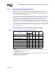
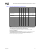
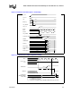
Table 22. Platform Power-On Timings
T# Parameter Min Max Unit Figure Notes
2
T45: Valid Time Before VTT_PWRGD 1.0 mS 14 1
T46: Valid Time Before PWRGOOD 2.0 mS 14 1
T47: RESET# Inactive to Valid Outputs 1 BCLK 14 1
T48: RESET# Inactive to Drive Signals 4 BCLK 14 1
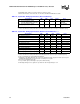
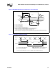
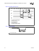
Figure 9. Clock Waveform
Vih
BCLK#
BCLK
Vil
Vcross
Tp
Tp = T1 (BCLK Period)
NOTE: Single-Ended clock uses BCLK only,
Differential clock uses BLCK and BCLK#