
Intel Celeron Processor in the 478-Pin Package at 1.80 GHz Datasheet

Datasheet 77
Intel
®
Celeron
®
Processor in the 478-Pin Package
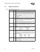
RESET# Input
Asserting the RESET# signal resets the processor to a known state and
invalidates its internal caches without writing back any of their contents. For a
power-on Reset, RESET# must stay active for at least one millisecond after V
CC
and BCLK have reached their proper specifications. On observing active
RESET#, all system bus agents will deassert their outputs within two clocks.
RESET# must not be kept asserted for more than 10 ms while PWRGOOD is
asserted.
A number of bus signals are sampled at the active-to-inactive transition of
RESET# for power-on configuration. These configuration options are described in
the Section 7.1.
This signal does not have on-die termination and must be terminated on the
system board.
RS[2:0]# Input
RS[2:0]# (Response Status) are driven by the response agent (the agent
responsible for completion of the current transaction), and must connect the
appropriate pins of all processor system bus agents.
RSP# Input
RSP# (Response Parity) is driven by the response agent (the agent responsible
for completion of the current transaction) during assertion of RS[2:0]#, the signals
for which RSP# provides parity protection. It must connect to the appropriate pins
of all processor system bus agents.
A correct parity signal is high if an even number of covered signals are low and
low if an odd number of covered signals are low. While RS[2:0]# = 000, RSP# is
also high, since this indicates it is not being driven by any agent guaranteeing
correct parity.
SKTOCC# Output
SKTOCC# (Socket Occupied) will be pulled to ground by the processor. System
board designers may use this pin to determine if the processor is present.
SLP# Input
SLP# (Sleep), when asserted in Stop-Grant state, causes the processor to enter
the Sleep state. During Sleep state, the processor stops providing internal clock
signals to all units, leaving only the Phase-Locked Loop (PLL) still operating.
Processors in this state will not recognize snoops or interrupts. The processor will
recognize only assertion of the RESET# signal, deassertion of SLP#, and
removal of the BCLK input while in Sleep state. If SLP# is deasserted, the
processor exits Sleep state and returns to Stop-Grant state, restarting its internal
clock signals to the bus and processor core units. If the BCLK input is stopped
while in the Sleep state the processor will exit the Sleep state and transition to the
Deep Sleep state.
SMI# Input
SMI# (System Management Interrupt) is asserted asynchronously by system
logic. On accepting a System Management Interrupt, the processor saves the
current state and enter System Management Mode (SMM). An SMI Acknowledge
transaction is issued, and the processor begins program execution from the SMM
handler.
If SMI# is asserted during the deassertion of RESET#, the processor will tristate
its outputs.
STPCLK# Input
STPCLK# (Stop Clock), when asserted, causes the processor to enter a low
power Stop-Grant state. The processor issues a Stop-Grant Acknowledge
transaction, and stops providing internal clock signals to all processor core units
except the system bus and APIC units. The processor continues to snoop bus
transactions and service interrupts while in Stop-Grant state. When STPCLK# is
deasserted, the processor restarts its internal clock to all units and resumes
execution. The assertion of STPCLK# has no effect on the bus clock; STPCLK#
is an asynchronous input.
TCK Input
TCK (Test Clock) provides the clock input for the processor Test Bus (also known
as the Test Access Port).
TDI Input
TDI (Test Data In) transfers serial test data into the processor. TDI provides the
serial input needed for JTAG specification support.
TDO Output
TDO (Test Data Out) transfers serial test data out of the processor. TDO provides
the serial output needed for JTAG specification support.
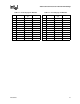
Table 32. Signal Description (Sheet 6 of 7)
Name Type Description