
Intel Celeron Processor in the 478-Pin Package at 1.80 GHz Datasheet

18 Datasheet
Intel
®
Celeron
®
Processor in the 478-Pin Package
2.4 Reserved, Unused, and TESTHI Pins
All RESERVED pins must remain unconnected. Connection of these pins to VCC, VSS, or to any
other signal (including each other) can result in component malfunction or incompatibility with a
future Celeron
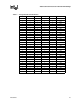
processors in the 478-pin package. See Chapter 5.0 for a pin listing of the processor
and the location of all RESERVED pins.
For reliable operation, always connect unused inputs or bidirectional signals to an appropriate
signal level. In a system level design, on-die termination has been included on the Celeron
processor in the 478-pin package to allow signals to be terminated within the processor silicon.
Most unused AGTL+ inputs should be left as no connects, as AGTL+ termination is provided on
the processor silicon. However, see Table 3 for details on AGTL+ signals that do not include on-die
termination. Unused active high inputs should be connected through a resistor to ground (V
SS).
Unused outputs can be left unconnected, however this may interfere with some TAP functions,
complicate debug probing, and prevent boundary scan testing. A resistor must be used when tying
bidirectional signals to power or ground. When tying any signal to power or ground, a resistor will
also allow for system testability. For unused AGTL+ input or I/O signals, use pull-up resistors of
the same value for the on-die termination resistors (R
TT
). See Table 12.
TAP, Asynchronous GTL+ inputs, and Asynchronous GTL+ outputs do not include on-die
termination. Input and used outputs must be terminated on the system board. Unused outputs may
be terminated on the system board or left unconnected. Note that leaving unused output
unterminated may interfere with some TAP functions, complicate debug probing, and prevent
boundary scan testing. Signal termination for these signal types is discussed in the appropriate
Platform Design Guide
, and the ITP700 Debug Port Design Guide.
The TESTHI pins should be tied to the processor V
CC using a matched resistor, where a matched
resistor has a resistance value within ± 20% of the impedance of the board transmission line traces.
For example, If the trace impedance is 50
Ω, then a value between 40 Ω and 60 Ω is required.
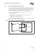
The TESTHI pins may use individual pull-up resistors or be grouped together as detailed below. A
matched resistor should be used for each group:
• TESTHI[1:0]
• TESTHI[5:2]
• TESTHI[10:8]
• TESTHI[12:11]
Additionally, if the ITPCLKOUT[1:0] pins are not used (see Table 32), they may be connected
individually to V
CC using matched resistors or grouped with TESTHI[5:2] with a single matched
resistor. If they are being used, individual termination with 1 k
Ω resistors is acceptable. Tying
ITPCLKOUT[1:0] directly to V
CC or sharing a pull-up resistor to VCC will prevent use of debug
interposers. This implementation is strongly discouraged for system boards that do not implement
an onboard debug port.
As an alternative, group 2 (TESTHI [5:2]), and the ITPCLKOUT[1:0] pins may be tied directly to
the processor V
CC. This has no impact on system functionality. TESTHI[0] and TESTHI[12] may
also be tied directly to processor V
CC if resistor termination is a problem, but matched resistor
termination is recommended. In the case of the ITPCLKOUT[1:0], direct tie to V
CC is strongly
discouraged for system boards that do not implement an onboard debug port.