
Intel Celeron Processor for the PGA370 Socket up to 1.40 GHz on 0.13 Micron Process Datasheet

Datasheet 25
Intel
®
Celeron
®
Processor for PGA370 up to 1.40 GHz on 0.13 µ Process
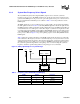
2.9 Test Access Port (TAP) Connection
Due to the voltage levels supported by other components in the Test Access Port (TAP) logic, it is
recommended that the processor be first in the TAP chain and followed by any other components
within the system. A translation buffer should be used to connect to the rest of the chain unless one
of the other components is capable of accepting an input of the appropriate voltage. Similar
considerations must be made for TCK, TMS, and TRST#. Two copies of each signal may be
required with each driving a different voltage level.
2.10 Maximum Ratings
Table 6 contains processor stress ratings only. Functional operation at the absolute maximum and
minimum is not implied nor guaranteed. The processor should not receive a clock while subjected
to these conditions. Functional operating conditions are given in the timing and level tables in
Section 2.11 through Section 2.13. Extended exposure to the maximum ratings may affect device
reliability. Furthermore, although the processor contains protective circuitry to resist damage from
static electric discharge, one should always take precautions to avoid high static voltages or electric
fields.
NOTES:
1. Input voltage can never exceed VSS +1.78 volts.
2. Input voltage can never exceed V
SS + 2.08 volts.
3. Input voltage can never go below -0.3 V
4. Parameter applies to CMOS, APIC, and TAP bus signal groups only.
2.11 Processor Voltage Level Specifications
The processor voltage level specifications in this section are defined at the PGA370 socket pins
(bottom side of the motherboard). See Section 7.0 for the processor signal descriptions and
Section 5.4 for the signal listings.
Most of the signals on the processor system bus are in the AGTL signal group. These signals are
specified to be terminated to 1.25 V. The voltage level specifications for these signals are listed in
Table 10 on page 29.
To allow connection with other devices, the clock, CMOS, APIC, and TAP signals are designed to
interface at non-AGTL levels. The voltage level specifications for these pins are listed in Table 11
on page 29.
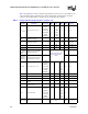
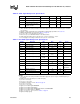
Table 6. Absolute Maximum Ratings
Symbol Parameter Min Max Unit Notes
TSTORAGE Processor storage temperature -40 85 °C
V
CC
CORE
and
V
TT
Processor core voltage and termination
supply voltage with respect to VSS
0.5 1.75 V
V
in
AGTL
AGTL buffer input voltage -0.3 1.78 V 1, 3
V
in
CMOS
1.5
CMOS buffer DC input voltage with respect
to V
SS
-0.3 2.08 V 2, 3, 4
V
VID & VBSEL Max VID and BSEL pin current -0.3 3.6 V