
Intel Celeron Processor in the 478-Pin Package at 1.80 GHz Datasheet

36 Datasheet
Intel
®
Celeron
®
Processor in the 478-Pin Package
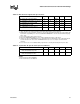
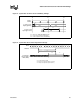
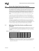
Figure 10. Source Synchronous 2X (Address) Timings
T
J
BCLK0
BCLK1
ADSTB# (@ driver)
A# (@ driver)
A# (@ receiver)
ADSTB# (@ receiver)
T1 T2
2.5 ns 5.0 ns 7.5 ns
T
H
T
H
T
J
T
N
T
K
T
M
valid valid
valid
valid
T
H
= T23: Source Sync. Address Output Valid Before Address Strobe
T
J
= T24: Source Sync. Address Output Valid After Address Strobe
T
K
= T27: Source Sync. Input Setup to BCLK
T
M
= T26: Source Sync. Input Hold Time
T
N
= T25: Source Sync. Input Setup Time
T
P
= T28: First Address Strobe to Second Address Strobe
T
S
= T20: Source Sync. Output Valid Delay
T
R
= T31: Address Strobe Output Valid Delay
T
P
T
R
T
S