
Intel Celeron Processor on 0.13 Micron Process in the 478-Pin Package Datasheet

Intel
®
Celeron
®
Processor on 0.13 Micron Process in the 478-Pin Package Datasheet 31
Electrical Specifications
Table 19. Miscellaneous Signals AC Specifications
T# Parameter Min Max Unit Figure Notes
1, 2, 3, 4
NOTES:
1. Unless otherwise noted, all specifications in this table apply to all processor frequencies.
2. All AC timings for the Asynch GTL+ signals are referenced to the BCLK0 rising edge at Crossing Voltage.
All Asynch GTL+ signal timings are referenced at GTLREF. PWRGOOD is referenced to the BCLK0 rising
edge at 0.5 * VCC.
3. These signals may be driven asynchronously.
4. See Section 7.2 for additional timing requirements for entering and leaving the low power states.
T35: Asynch GTL+ Input Pulse Width 2 BCLKs
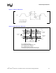
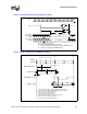
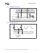
T36: PWRGOOD to RESET# deassertion time 1 10 ms 14
T37: PWRGOOD Inactive Pulse Width 10 BCLKs 14
5
5. Refer to the PWRGOOD definition for more details regarding the behavior of this signal.
T38: PROCHOT# pulse width 500 µs 15
6
6. Length of assertion for PROCHOT# does not equal TCC activation time. The processor requires time to en-
able or disable the TCC after the assertion or deassertion of PROCHOT#. Additionally, time is allocated after
the assertion or deassertion of PROCHOT# for the processor to complete current instruction execution. This
specification applies to PROCHOT# as both an input and an output.
T39: THERMTRIP# to VCC Removal 0.5 s 17
T40: FERR# Valid Delay from STPCLK# deassertion 0 5 BCLKs Section 3
Table 20. System Bus AC Specifications (Reset Conditions)
T# Parameter Min Max Unit Figure Notes
T45: Reset Configuration Signals (A[31:3]#, BR0#,
INIT#, SMI#) Setup Time
4 BCLKs 11
1
NOTES:
1. Before the deassertion of RESET#.
T46: Reset Configuration Signals (A[31:3]#, INIT#,
SMI#) Hold Time
2 20 BCLKs 11
2
2. After clock that deasserts RESET#.
T47: Reset Configuration Signal BR0# Hold Time 2 2 BCLKs 11
2
Table 21. TAP Signals AC Specifications
Parameter Min Max Unit Figure Notes
1, 2, 3
NOTES:
1. Unless otherwise noted, all specifications in this table apply to all processor frequencies.
2. Not 100% tested. Specified by design characterization.
3. All AC timings for the TAP signals are referenced to the TCK signal at 0.5*VCC at the processor pins. All TAP
signal timings (TMS, TDI, etc) are referenced at 0.5*VCC at the processor pins.
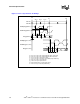
T55: TCK Period 60.0 ns 7
T56: TCK Rise Time 10.0 ns 7
4
4. Rise and fall times are measured from the 20% to 80% points of the signal swing.
T57: TCK Fall Time 10.0 ns 7
4
T58: TMS Rise Time 8.5 ns 7
4
T59: TMS Fall Time 8.5 ns 7
4, 5
5. It is recommended that TMS be asserted while TRST# is being deasserted.
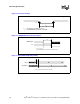
T61: TDI Setup Time 0 ns 20
6,
7
6. Referenced to the rising edge of TCK.
7. Specifications for a minimum swing defined between TAP VT- to VT+. This assumes a minimum edge rate
of 0.5 V/ns.
T62: TDI Hold Time 3 ns 20
6, 7
T63: TDO Clock to Output Delay 3.5 ns 20
6
T64: TRST# Assert Time 2 TCK 16
8,
5
8. TRST# must be held asserted for 2 TCK periods to be guaranteed that it is recognized by the processor.