
Intel Celeron Processor on 0.13 Micron Process in the 478-Pin Package Datasheet

30 Intel
®
Celeron
®
Processor on 0.13 Micron Process in the 478-Pin Package Datasheet
Electrical Specifications
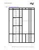
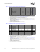
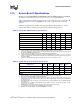
Table 18. System Bus Source Synch AC Specifications AGTL+ Signal Group
T# Parameter Min Typ Max Unit Figure Notes
1, 2, 3, 4
NOTES:
1. Unless otherwise noted, all specifications in this table apply to all processor frequencies and cache sizes.
2. Not 100% tested. Specified by design characterization.
3. All source synchronous AC timings are referenced to their associated strobe at GTLREF. Source synchro-
nous data signals are referenced to the falling edge of their associated data strobe. Source synchronous ad-
dress signals are referenced to the rising and falling edge of their associated address strobe. All source
synchronous AGTL+ signal timings are referenced to GTLREF at the processor core.
4. Unless otherwise noted, these specifications apply to both data and address timings.
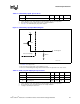
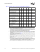
T20: Source Synchronous Data Output
Valid Delay (first data/address only)
0.20 1.20 ns 12, 13
5
5. Valid delay timings for these signals are specified into the test circuit described in Figure 6 and with GTLREF.
T21: T
VBD
: Source Synchronous Data
Output Valid Before Strobe
0.85 ns 13
5,
6
6. This specification represents the minimum time the data or address will be valid before its strobe. Refer to
the appropriate Platform Design Guide listed in
Table 1 for more information on the definitions and use of these
specifications.
T22: T
VAD
: Source Synchronous Data
Output Valid After Strobe
0.85 ns 13
5,
6
T23: T
VBA
: Source Synchronous
Address Output Valid Before Strobe
1.88 ns 12
5,
6
T24: T
VAA
: Source Synchronous
Address Output Valid After Strobe
1.88 ns 12
5,
7
7. This specification represents the minimum time the data or address will be valid after its strobe. Refer to the
appropriate Platform Design Guide listed in
Table 1.
T25: T
SUSS
: Source Synchronous Input
Setup Time to Strobe
0.21 ns 12, 13
8
8. Specification is for a minimum swing defined between AGTL+ V
IL_MAX
to V
IH_MIN
. This assumes an edge rate
of 0.3 V/ns to 4.0 V/ns.
T26: T
HSS
: Source Synchronous Input
Hold Time to Strobe
0.21 ns 12, 13
8
T27: T
SUCC
: Source Synchronous Input
Setup Time to BCLK[1:0]
0.65 ns 12, 13
9
9. All source synchronous signals must meet the specified setup time to BCLK as well as the setup time to each
respective strobe.
T28: T
FASS
: First Address Strobe to
Second Address Strobe
1/2 BCLK 12
10
10. The rising edge of ADSTB# must come approximately 1/2 BCLK period (5 ns) after the falling edge of AD-
STB#.
T29: T
FDSS
: First Data Strobe to
Subsequent Strobes
n/4 BCLK 13
11,
12
11. For this timing parameter, n = 1, 2, and 3 for the second, third, and last data strobes respectively.
12. The second data strobe (falling edge of DSTBN#) must come approximately 1/4 BCLK period (2.5 ns) after
the first falling edge of DSTBp#. The third data strobe (falling edge of DSTBp#) must come approximately
2/4 BCLK period (5 ns) after the first falling edge of DSTBp#. The last data strobe (falling edge of DSTBn#)
must come approximately 3/4 BCLK period (7.5 ns) after the first falling edge of DSTBp#.
T30: Data Strobe ‘n’ (DSTBN#) Output
valid Delay
8.80 10.20 ns 13
13
13. This specification applies only to DSTBN[3:0]# and is measured to the second falling edge of the strobe.
T31: Address Strobe Output Valid Delay 2.27 4.23 ns 12