
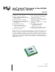
Intel Celeron Processor in the 478-Pin Package at 1.80 GHz Datasheet


Datasheet 9
Intel
®
Celeron
®
Processor in the 478-Pin Package
1.0 Introduction
The Intel
®
Celeron
®
processor in the 478-pin package utilizes Flip-Chip Pin Grid Array
(FC-PGA2) package technology, and plugs into a 478-pin surface mount, Zero Insertion Force
(ZIF) socket, referred to as the mPGA478B socket. The Celeron
processor in the 478-pin package
maintains the tradition of compatibility with IA-32 software.
The Celeron
processor in the 478-pin package is designed for uni-processor based Value PC
desktop systems. Features of processor include hyper pipelined technology, a 400 MHz system bus,
and an execution trace cache. The 400 MHz system bus is a quad-pumped bus that is clocked with
a 100 MHz system clock, making 3.2 GB/sec data transfer rates possible. The execution trace
cache is a first level cache that stores approximately 12k decoded micro-operations, which removes
the decoder from the main execution path.
Additional features include advanced dynamic execution, advanced transfer cache, enhanced
floating point and multi-media unit, and Streaming SIMD Extensions 2 (SSE2). The advanced
dynamic execution improves speculative execution and branch prediction internal to the processor.
The advanced transfer cache is a 128 KB, on-die level 2 (L2) cache. The floating point and multi-
media units have 128 bit wide registers with a separate register for data movement. Finally, SSE2
support includes instructions for double-precision floating point, SIMD integer, and memory
management. Power management capabilities such as AutoHALT, Stop-Grant, Sleep, and Deep
Sleep have also been retained.
The Celeron
processor in the 478-pin package 400 MHz system bus utilizes a split-transaction,
deferred reply protocol. This system bus is not compatible with the P6 processor family bus. The
400 MHz system bus uses Source-Synchronous Transfer (SST) of address and data to improve
throughput by transferring data four times per bus clock (4X data transfer rate, as in AGP 4X).
Along with the 4X data bus, the address bus can deliver addresses two times per bus clock, and is
referred to as a “double-clocked” or 2X address bus. Working together, the 4X data bus and 2X
address bus provide a data bus bandwidth of up to 3.2 GB/second.
Intel will be enabling support components for the Celeron
processor in the 478-pin package
including a heatsink, heat sink retention mechanism, and socket. Manufacturability is a high
priority; hence mechanical assembly can be completed from the top of the motherboard and should
not require any special tooling. The processor system bus uses a variant of GTL+ signalling
technology called Assisted Gunning Transceiver Logic (AGTL+) signalling technology.
1.1 Terminology
A “#” symbol after a signal name refers to an active low signal, indicating a signal is in the active
state when driven to a low level. For example, when RESET# is low, a reset has been requested.
Conversely, when NMI is high, a nonmaskable interrupt has occurred. In the case of signals where
the name does not imply an active state but describes part of a binary sequence (such as address or
data), the “#” symbol implies that the signal is inverted. For example, D[3:0] = “HLHL” refers to a
hex “A”, and D[3:0]# = “LHLH” also refers to a hex “A” (H= High logic level, L= Low logic
level).
System Bus refers to the interface between the processor and system core logic (a.k.a. the chipset
components). The system bus is a multiprocessing interface for processors, memory, and I/O.