
Guide

Platform Design Checklist
R
Intel
®
852GM Chipset Platform Design Guide 255
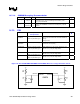
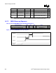
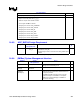
Table 99. GST[1:0] Configurations
GMCH GST[1:0]
Configuration
FSB DDR
Gfx Core Clock Low Gfx Core Clock High
00 400 266 N/a 133
10 400 200 N/a 133
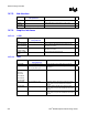
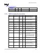
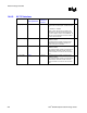
14.7.6. GMCH Decoupling Recommendations
Pin Name Configuration F Qty Notes
9
VCC Connect to Vcc1_2 0.1 µF
150 µF
10 µF
4
2
1
Bulk decoupling is based on VR
solutions used on CRB design.
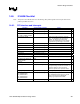
VTTLF Connect to VCCP 0.1 µF
150 µF
10 µF
2
1
1
Bulk decoupling is based on VR
solutions used on CRB design.
VTTHF 0.1 µF 5 Connect pins directly to caps.
VCCHL Connect to Vcc1_2 0.1 µF
10 µF
2
1
Bulk decoupling is based on VR
solutions used on CRB design.
VCCSM Connect to
VccSus2_5
0.1 µF
150 µF
11
2
Bulk decoupling is based on VR
solutions used on CRB design.
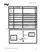
VCCQSM Connect to
VccSus2_5 with
filter network
0.1 µF
4.7 µF+1
Ω
1
1 each
0.68 µH from power supply to GMCH
pins. On GMCH side of inductor: one 0.1
µF to GND, 4.7 µF + 1
Ω to GND
VCCASM Connect to Vcc1_2
with filter network
0.1 µF
100 µF
1
1
1 µH from power supply to GMCH pins,
with caps on GMCH side of inductor.
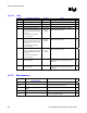
VCCDVO Connect to Vcc1_5 0.1 µF
10 µF
150 µF
2
1
1
Bulk decoupling is based on VR
solutions used on CRB design.
VCCADAC Connect to Vcc1_5 0.01 µF
0.1 µF
220 µF (no
stuff)
1
1
1
Route VSSADAC to other side of the
caps, then to ground.
A 0-ohm 0805 resisor is recommended
between the caps and Vcc1_5. This and
the 220 µF cap footprints are there in
case there is noise issue with the VGA
supply.
VCCALVDS Connect to Vcc1_5 0.1 µF
0.01 µF
1
1
Route VSSALVDS to other side of the
caps, then to ground.
VCCDLVDS Connect to Vcc1_5 0.1 µF
22 µF
47 µF
1
1
1
Bulk decoupling is based on VR
solutions used on CRB design.
VCCTXLVDS
Connect to
VccSus2_5
0.1 µF
22 µf
47 µF
3
1
1
Bulk decoupling is based on VR
solutions used on CRB design.
This power signal may be optionally
connected to Vcc2_5 and powered off in
S3.
VCCGPIO Connect to Vcc3_3 0.1 µF
10 µF
1
1
Bulk decoupling is based on VR
solutions used on CRB design.