
Intel Celeron Processor in the 478-Pin Package at 1.80 GHz Datasheet


Datasheet 39
Intel
®
Celeron
®
Processor in the 478-Pin Package
3.0 System Bus Signal Quality Specifications
Source synchronous data transfer requires the clean reception of data signals and their associated
strobes. Ringing below receiver thresholds, non-monotonic signal edges, and excessive voltage
swing will adversely affect system timings. Ringback and signal non-monotinicity cannot be
tolerated since these phenomena may inadvertently advance receiver state machines. Excessive
signal swings (overshoot and undershoot) are detrimental to silicon gate oxide integrity, and can
cause device failure if absolute voltage limits are exceeded. Additionally, overshoot and
undershoot can cause timing degradation due to the build up of inter-symbol interference (ISI)
effects.
For these reasons, it is important that the designer work to achieve a solution that provides
acceptable signal quality across all systematic variations encountered in volume manufacturing.
This section documents signal quality metrics used to derive topology and routing guidelines
through simulation, and all specifications are at the processor silicon and cannot be measured at the
processor pins.
Specifications for signal quality are for measurements at the processor core only and are only
observable through simulation. The same is true for all system bus AC timing specifications in
Section 2.12. Therefore, proper simulation of the Celeron
processor in the 478-pin package system
bus is the only means to verify proper timing and signal quality metrics, and Intel highly
recommends simulation during system design and measurement during system analysis.
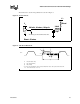
3.1 BCLK Signal Quality Specifications and Measurement
Guidelines
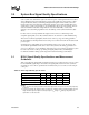
Table 19 describes the signal quality specifications at the processor silicon for the processor system
bus clock (BCLK) signals. Figure 16 describes the signal quality waveform for the system bus
clock at the processor silicon. Specifications are defined at the processor silicon, not the 478-pin
socket pins.
NOTES:
1. Unless otherwise noted, all specifications in this table apply to all Celeron processor in the 478-pin package
frequencies.
2. The rising and falling edge ringback voltage specified is the minimum (rising) or maximum (falling) absolute
voltage the BCLK signal can dip back to after passing the V
IH
(rising) or V
IL
(falling) voltage limits. This
specification is an absolute value.
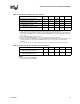
Table 19. BCLK Signal Quality Specifications
Parameter Min Max Unit Figure Notes
1
BCLK[1:0] Overshoot N/A 0.30 V 16
BCLK[1:0] Undershoot N/A 0.30 V 16
BCLK[1:0] Ringback Margin 0.20 N/A V 16
BCLK[1:0] Threshold Region N/A 0.20 V 16 2