
Intel Celeron Processor in the 478-Pin Package at 1.80 GHz Datasheet

32 Datasheet
Intel
®
Celeron
®
Processor in the 478-Pin Package
NOTES:
1. Unless otherwise noted, all specifications in this table apply to all processor frequencies.
2. Not 100% tested. Specified by design characterization.
3. All AC timings for the TAP signals are referenced to the TCK signal at 0.5 V
CC at the processor pins. All TAP
signal timings (TMS, TDI, etc) are referenced at 0.5 * V
CC at the processor pins.
4. Rise and fall times are measured from the 20% to 80% points of the signal swing.
5. Referenced to the rising edge of TCK.
6. Referenced to the falling edge of TCK.
7. Specification for a minimum swing defined between TAP 20%
to 80% points on the waveform. This assumes
a minimum edge rate of 0.5 V/ns.
8. TRST# must be held asserted for 2 TCK periods to be guarantee that it is recognized by the processor.
9. It is recommended that TMS be asserted while TRST# is being deasserted.
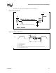
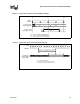
2.13 Processor AC Timing Waveforms
The following figures are used in conjunction with the AC timing tables, Table 14 through
Table 18.
Note: For Figure 5 through Figure 14, the following apply:
• All common clock AC timings for AGTL+ signals are referenced to the Crossing Voltage
(V
CROSS
) of the BCLK[1:0] at rising edge of BCLK0. All common clock AGTL+ signal
timings are referenced at GTLREF at the processor core.
• All source synchronous AC timings for AGTL+ signals are referenced to their associated
strobe (address or data) at GTLREF. Source synchronous data signals are referenced to the
falling edge of their associated data strobe. Source synchronous address signals are referenced
to the rising and falling edge of their associated address strobe. All source synchronous
AGTL+ signal timings are referenced at GTLREF at the processor silicon.
• All AC timings for AGTL+ strobe signals are referenced to BCLK[1:0] at V
CROSS
. All
AGTL+ strobe signal timings are referenced at GTLREF at the processor silicon.
• All AC timings for the TAP signals are referenced to the TCK signal at 0.5 * VCC at the
processor pins. All TAP signal timings (TMS, TDI, etc) are referenced at 0.5 * V
CC at the
processor pins.
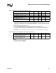
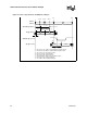
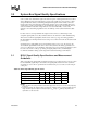
Table 18. TAP Signals AC Specifications
Parameter Min Max Unit Figure Notes
1,2,3,9
T55: TCK Period 60.0 ns 5
T56: TCK Rise Time 9.5 ns 5 4
T57: TCK Fall Time 9.5 ns 5 4
T58: TMS, TDI Rise Time 8.5 ns 5 4
T59: TMS, TDI Fall Time 8.5 ns 5 4
T61: TDI, TMS Setup Time 0 ns 15 5, 7
T62: TDI, TMS Hold Time 3 ns 15 5, 7
T63: TDO Clock to Output Delay 0.5 3.5 ns 15 6
T64: TRST# Assert Time 2 TCK 14 8