
Intel Celeron Processor in the 478-Pin Package at 1.80 GHz Datasheet


Datasheet 29
Intel
®
Celeron
®
Processor in the 478-Pin Package
.
NOTES:
1. Unless otherwise noted, all specifications in this table apply to all processor frequencies.
2. Not 100% tested. Specified by design characterization.
3. All common clock AC timings for AGTL+ signals are referenced to the Crossing Voltage (V
CROSS
) of the
BCLK[1:0] at rising edge of BCLK0. All common clock AGTL+ signal timings are referenced at GTLREF at the
processor core.
4. Valid delay timings for these signals are specified into the test circuit described in Figure 4 and with GTLREF
at 2/3 V
CC ± 2%.
5. Specification is for a minimum swing defined between AGTL+ V
IL_MAX
to V
IH_MIN
. This assumes an edge rate
of 0.4 V/ ns to 4.0 V/ns.
6. RESET# can be asserted asynchronously, but must be deasserted synchronously.
7. This should be measured after V
CC and BCLK[1:0] become stable.
8. Maximum specification applies only while PWRGOOD is asserted.
.
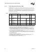
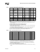
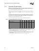
Table 14. System Bus Common Clock AC Specifications
T# Parameter Min Max Unit Figure Notes
1,2,3
T10: Common Clock Output Valid Delay 0.200 1.45 ns 8 4
T11: Common Clock Input Setup Time 0.65 N/A ns 8 5
T12: Common Clock Input Hold Time 0.40 N/A ns 8 5
T13: RESET# Pulse Width 1.00 10.00 ms 9 6, 7, 8