
Intel Celeron Processor in the 478-Pin Package at 1.80 GHz Datasheet


20 Datasheet
Intel
®
Celeron
®
Processor in the 478-Pin Package
2.6 Asynchronous GTL+ Signals
The Celeron
processor in the 478-pin package does not utilize CMOS voltage levels on any signals
that connect to the processor. As a result, legacy input signals such as A20M#, IGNNE#, INIT#,
LINT0/INTR, LINT1/NMI, SMI#, SLP#, and STPCLK# utilize GTL+ input buffers. Legacy
output FERR# and other non-AGTL+ signals (THERMTRIP# and PROCHOT#) utilize GTL+
output buffers. All of these signals follow the same DC requirements as AGTL+ signals, however
the outputs are not actively driven high (during a logical 0 to 1 transition) by the processor (the
major difference between GTL+ and AGTL+). These signals do not have setup or hold time
specifications in relation to BCLK[1:0]. However, all of the Asynchronous GTL+ signals are
required to be asserted for at least two BCLKs in order for the processor to recognize them. See
Section 2.10 and Section 2.12 for the DC and AC specifications for the Asynchronous GTL+ signal
groups. See Section 7.2 for additional timing requirements for entering and leaving the low power
states.
2.7 Test Access Port (TAP) Connection
Due to the voltage levels supported by other components in the Test Access Port (TAP) logic, it is
recommended that the Celeron
processor in the 478-pin package be first in the TAP chain and
followed by any other components within the system. A translation buffer should be used to
connect to the rest of the chain unless one of the other components is capable of accepting an input
of the appropriate voltage level. These considerations must be made for TCK, TMS, TRST#, TDI,
and TDO. Two copies of each signal may be required, with each driving a different voltage level.
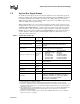
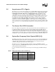
2.8 System Bus Frequency Select Signals (BSEL[1:0])
The BSEL[1:0] signals are used to select the frequency of the processor input clock (BCLK[1:0]).
Table 4 defines the possible combinations of the signals and the frequency associated with each
combination. The required frequency is determined by the processor, chipset, and clock
synthesizer. All agents must operate at the same frequency.
The Celeron
processor in the 478-pin package currently operates at a 400 MHz system bus
frequency (selected by a 100 MHz BCLK[1:0] frequency). Individual processors will only operate
at their specified system bus frequency.
For more information about these pins refer to Chapter 5.0 and the appropriate Platform Design
Guide.
Table 4. BSEL[1:0] Frequency Table for BCLK[1:0]
BSEL1 BSEL0 Function
L L 100 MHz
LHRESERVED
HLRESERVED
HHRESERVED