
Guide
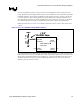
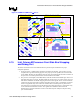

Intel Celeron M Processor Front Side Bus Design Guidelines
R
80 Intel
®
852GM Chipset Platform Design Guide
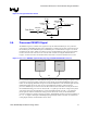
Table 29. ITP Signal Default Strapping When ITP Debug Port Not Used
Signal Resistor Value Connect To Resistor Placement
TDI 150 Ω ± 5% VCCP Within 2.0” of the CPU
TMS 39 Ω ± 5% VCCP Within 2.0” of the CPU
TRST# 680 Ω ± 5% GND Within 2.0” of the CPU
TCK 27 Ω ± 5% GND Within 2.0” of the CPU
TDO Open NC N/A
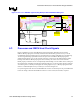
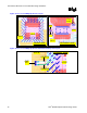
5.11. Processor V
CCSENSE
/V
SSSENSE
Design Recommendations
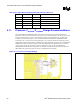
The VCCSENSE and VSSSENSE signals of the Intel Celeron M Processor provide isolated, low
impedance connections to the processor’s core power (VCC) and ground (VSS). These pins can be used
to sense or measure power (VCC) or ground (VSS) near the silicon with little noise. To make them
available for measurement purposes, it is recommended that VCCSENSE and VSSSENSE both be
routed with a Zo = 55 Ω ± 15% trace of equal length. Use 3:1 spacing between the routing for the two
signals and all other signals should be a minimum of 25 mils (preferably 50 mils) from VCCSENSE and
VSSSENSE routing. Terminate each line with an optional (default is No Stuff) 54.9 Ω ± 1% resistor.
Also, a ground via spaced 100 mils away from each of the test point vias for VCCSENSE and
VSSSENSE should be added. A third ground via should also be placed in between them to allow for a
differential probe ground. See Figure 42 for the recommended layout example.
Figure 42. V
CCSENSE
/V
SSSENSE
Routing Example